High-Purity Sublimed Materials for Organic Electronic Devices
Thin Film Transistor Device Preparation and Performance using Triple-Sublimed Pentacene
Introduction
Organic field-effect transistors (OFETs) have attracted considerable attention due to their potential for realizing large-area, mechanically flexible, lightweight and low-cost devices. One of the key components for performance in these devices is the organic semiconductor, and as such the design and purity of new semiconductor materials has been critical to the advancement of organic electronics technology. The highest mobility devices demonstrated in the literature have utilized small molecule semiconductors,1 (as shown in the single crystal device2 – Figure 1) or a blend of small molecule and polymer materials.3

Figure 1.Sublimed grade Rubrene (551112) in a single-crystal OFET setup2, with an extremely high hole mobility of ~8 cm2/V.s.
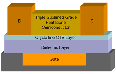
High purity organic semiconductor material is preferable to achieve better properties (hole mobility and on/off ratio) in organic thin film transistors (OTFTs) and may help increase the device lifetime. The sublimation technique is a very good purification method and because a number of organic semiconducting materials (i.e. pentacene) sublime at high temperatures and high vacuum, higher purity materials can be obtained. An OTFT device was fabricated using a triple-sublimed grade of pentacene (698423), and the ultra high performance characteristics are reported in this note.

Figure 2.Schematic of an OTFT device showing the dielectric layer modified with crystalline OTS and Triple-Sublimed pentacene as the semiconductor (698423).
Device Preparation and Characterization
Pentacene thin film transistors were fabricated using triple-sublimed ≥99.995 % purity pentacene as the active material. Heavily n-doped silicon substrates with a thermally grown 300 nm silicon dioxide dielectric layer, and a capacitance per unit area (Ci) of 10 nF/cm2 were used as transistor substrates (Silicon Quest Inc.). The Si/SiO2 was cleaned in piranha solution (7:3 H2SO4: H2O2 CAUTION: highly reactive) for 30 minutes and then copiously washed with deionized water. A crystalline monolayer of octadecylsilane (OTS) (442291) was then deposited on the Si/SiO2 wafer pieces to modify the dielectric surface. We have previously reported4 the details for the preparation of the crystalline OTS monolayer. Pentacene was then deposited via thermal evaporation at a rate of 0.3-0.4 Å/s, under a vacuum pressure of 10-6- 10-7 Torr with a substrate temperature of 60 ºC to obtain a final film thickness of 40 nm (as determined by a quartz crystal monitor in the evaporation chamber). Subsequently, gold electrodes (~40 nm in thickness) were deposited using shadow masks with a W/L of 20 (W = channel width, L = channel length), where L = 50-150 μm.
The electrical characteristics of the pentacene transistors were obtained at room temperature in ambient conditions using a Keithley 4200 (Hewlett-Packard) semiconductor parameter analyzer. Transfer current-voltage (IV) characteristics were obtained with a fixed source-drain voltage of -100 V.
Results
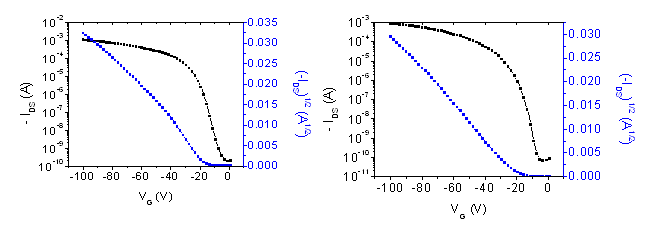
Representative transfer IV curves are shown below:

Figure 3.Representative transfer IV curves of OTFT devices (Left- Device #3 and Right- Device #5 in Table 1) with Triple sublimed pentacene (698423).

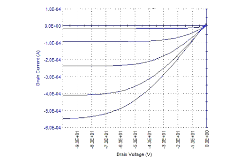
Figure 4.Output IV curves of a Triple-Sublimed pentacene (698423) OTFT (Device #1).
Note that the transfer curves in Figure 3, the on/off ratios are in excess of 106. The charge carrier mobility was calculated from the saturation transfer IV curves (Figure 4) using the relationship:
IDS = (WC/2L)µ (Vg - Vt)2
Where μ is the charge carrier mobility, IDS is the drain current, VG is the gate voltage , VT is the threshold voltage and C is the capacitance. The channel geometry is defined by the (channel width (W) and length (L)).
The key transistor metrics (mobility, on/off and threshold voltage) for seven OTFTs fabricated using Triple-Sublimed Pentacene are given below:
Summary
Pentacene organic thin film transistors (OTFTs) were fabricated using triple-sublimed ≥99.995 % purity pentacene. On crystalline octadecylsilane modified SiO2 dielectric surface the average charge carrier mobility was 3.4 cm2/Vs (max 4.6 cm2/Vs). The extremely high performance of the OTFTs is attributed to the high purity of the pentacene, and the crystalline dielectric modification layer.
We offer a selection of high-purity sublimed materials, suitable for a wide range of organic electronics applications. In order to consistently offer the highest quality materials, sublimed grade products are subject to extensive purity testing, which can include:
- Trace Metals Analysis
- DSC / TGA
- HPLC (if the material is soluble)
Product specific testing information can be found on the specification sheet or the Certificate of Analysis.
Materials
References
如要继续阅读,请登录或创建帐户。
暂无帐户?