Conductive Polymers for Advanced Micro- and Nano-fabrication Processes
Introduction
Conducting polymers such as polyaniline, polythiophene and polyfluorenes are now much in the spotlight for their applications in organic electronics and optoelectronics. Such materials are used, for example, in making organic thin-film transistors and light-emitting diodes. Here, we present a novel application of conductive polymer thin films – for use as charge dissipation layers for state-of-the-art patterning techniques, i.e., electron-beam lithography (EBL) and focused ion beam (FIB) etching, on demanding substrates. The ability of thin polythiophene layers to dissipate accumulated charge in electron-beam lithography of wide bandgap semiconductors, e.g., zinc oxide1 and gallium nitride2, as well as for focused ion beam patterning of glass is demonstrated here. The former technique (EBL) is related to the creation of dense periodic nanopatterns in hydrogen silsesquioxane (HSQ) negative-type e-beam resist, so that passive photonic devices could be fabricated in a semiconductor by a subsequent dry etch process. The latter technology (FIB etching) is related to biomedical applications as glass capillaries are routinely used in electrophysiological investigations of mammalian cells.3
In each case, we used commercially-available 2.5% aqueous dispersion of poly(3,4-ethylenedioxythiophene)-poly(styrenesulfonate) (PEDOT:PSS, Prod. No. 655201). The high electrical conductivity and good oxidation resistance of these polymer films make them suitable for electromagnetic shielding and noise suppression applications. The optical transmission spectrum of the polythiophene film deposited on a float glass substrate revealed a featureless transmission curve.2 Thus, the polymer film was found to possess high transparency throughout the visible light spectrum and even into near IR and near UV regions. In addition, values of extinction coefficient k for a thin polythiophene film are negligible in a wide range of wavelengths, including the visible light spectrum, as experimentally determined with the use of a rotating analyzer ellipsometer. The optical transparency of polythiophene charge dissipation layers makes it easy to see the sample surface and perform any alignment operations required to align patterns with pre-existing device features.
Sample Processing Using PEDOT:PSS Conductive Polymer
Conductive Polymers for Electron-beam Lithography (EBL)
A quick and inexpensive processing method has been developed for EBL exposure of dense and high-resolution patterns in hydrogen silsesquioxane (HSQ) negative-type resist deposited on bulk ZnO and on GaN/AlN-on-sapphire substrate. Zinc oxide (ZnO, Prod. No. 255750) is a wide bandgap semiconductor that is attracting much attention these days owing to its potential for fabricating blue light emitting devices, thin-film transistors (TFTs) and potentially even laser diodes. This II-VI oxide semiconductor has about the same bandgap (~3.4 eV) as gallium nitride (GaN, Prod. No. 481769) which is now the standard material for making short wavelength light emitting diodes and laser diodes. ZnO, however, is not just an alternative material but has a number of advantages over GaN when it comes to making similar devices. These include a higher exciton binding energy and the availability of bulk substrates. III-V-Nitride compounds (GaN, InN and AlN) are interesting and prospective materials for future optoelectronics applications. These new materials can be indispensable in violet and UV spectral regions, but they are also very useful for the generation and detection of blue and green light. All III-V nitrides have a direct energy band-gap, a valuable feature which increases their usefulness over indirect band-gap semiconductors for making both light emitters and light detectors. There is also the possibility of forming solid solutions with InN (Prod. No. 490628) and AlN (Prod. No. 241903), which allows tailoring optical and electrical properties. GaN also exhibits high mechanical and thermal stability, which makes it very useful for high-temperature electronic and optoelectronic applications such as power transistors, high power LEDs and lasers.
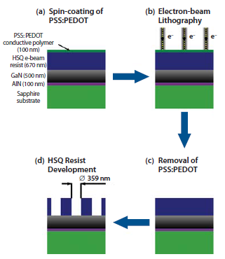
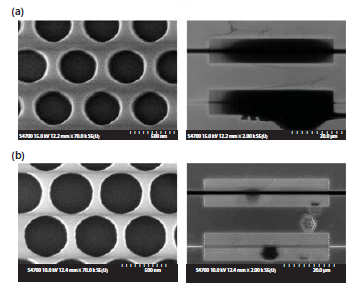
Both electron microscope inspection and electron-beam lithography patterning of ZnO and GaN face difficulties because these materials are not able to efficiently dissipate the charge that accumulates during such processes. Consequently, e-beam lithography of wide bandgap semiconductors is commonly performed with a thin conducting metal layer, usually aluminum, deposited on top of the e-beam resist. Furthermore, the processing of ZnO is difficult since it is an amphoteric oxide, which is easily attacked by both acids and bases, e.g., used for the removal of metal films. Here, we describe a much simpler technique, in comparison with metal layer evaporation. It can be widely used without any special resist preparation steps. The use of commercially available PEDOT:PSS conductive polymer to dissipate charge in electron-beam lithography is schematically presented in Figure 1, using an epitaxial GaN/AlN/sapphire sample. Processing involves spin-coating of a conductive polymer (PEDOT:PSS) on top of a HSQ-coated sample, electron-beam writing of dense patterns in resist, removal of the PEDOT: PSS layer and, finally, development of the exposed HSQ e-beam resist. Comparison of experimental results is given here for two different cases, where no charge dissipation layer was used, as well as the case where a 100-nm-thick conductive polymer layer was deposited on top of the HSQ resist (Figure 2). Scanning-electron microscope (SEM) observations of the resulting photonic crystal (PhC) patterns, exposed with the same dose of 442 μC/cm2, are shown in Figure 2, at two different magnifications 2k and 70k. The fabricated nano-patterns included a 50 μM × 10 μM area of pattern W1 (one row of holes removed) and W3 (three rows of holes removed) photonic crystal waveguide structures with a triangular lattice of holes (periodicity of 550 nm, designed hole diameter of 440 nm). For the pure HSQ case (Figure 2a) severe overexposure of the periodic pattern was observed. Despite properly defined holes on the edges of an array, the middle part of the PhC lattice exhibited signs of strong proximity effect, which is indicated by a decrease in SEM observation contrast. In the case where the conductive polymer was used, however, sharply defined holes were obtained within highly uniform photonic crystal lattices, as additionally indicated by high contrast SEM micrographs (Figure 2b).

Figure 1.Schematic presentation of the experimental HSQ/PEDOT:PSS/GaN/AlN/Al2O3 sample patterned by electron-beam lithography with the use of a conductive polymer charge dissipation layer: a) deposition of thin PEDOT:PSS film by a spin-coating technique; b) writing a pattern in HSQ resist with electron-beam-based process; c) removal of PEDOT:PSS in warm bath of deionised water; d) development of HSQ resist, dense nano-patterns are revealed in the resist layer.

Figure 2.Scanning-electron microscope (SEM) pictures (top-view) of a photonic crystal lattice in HSQ resist on bulk ZnO sample, for an e-beam exposure dose of 442 μC/cm2: a) e-beam exposure process without a conductive polymer used; b) e-beam exposure process with thin conductive polymer used.
After processing, spin-coatable conducting polymer may be easily removed due to its solubility in water, which makes it a perfect solution for the processing of amphoteric oxide samples, e.g., zinc oxide. Gallium nitride processing also benefits from polymer dissipation layer usage due to extended exposure range and the avoidance of dense pattern overexposure in HSQ. The new approach provides the ability to make ZnO and GaN sample processing much simpler, quicker, and less expensive, but it may also be extended to EBL exposures of many other semiconductor/dielectric materials, as described in the next paragraph.
Conductive Polymers for Focused Ion Beam (FIB) Etching
A water-soluble film formed by a PEDOT:PSS conductive polymer was also used to prevent electrical charging during ion milling of a glass material. Ion milling is performed using a tightly focused beam of ions to ablate material with nanometer precision. This is achieved as the beam positioning and the milling progress are both monitored in-situ with a scanning-electron microscope. In our experiments, glass capillaries were used as the target material to be patterned on microscale. Glass capillaries are commonly used in electrophysiological investigations of mammalian cells (e.g., microelectrodes for patch clamp), where the locally heated capillaries are pulled to form a tapered tip with an opening ranging from 1 μM to 100 μM in diameter. The tapered tip of a pulled capillary is routinely used for locally altering the concentration of a substance in solution in a spatially and temporarily defined manner.3 Glass capillaries can be pulled to form hollow filaments (~30 μM inner diameter) with thin walls (~5 to 10 μM thick). Perforation of these filaments at defined locations would enable the formation of two compartments (inside/outside of the capillary), communicating only through the openings in the capillary wall. With one end of the liquid-filled capillary pressurized and the other end closed one could use this arrangement to apply the liquid to predefined locations. This is because the openings in the capillary wall allow the liquid to leave the inside of the capillary and diffuse into the solution outside. To fabricate well-defined openings in a capillary wall a FIB patterning was used. A prerequisite of FIB processing is a conductive coating e.g., with a AuPd metal layer sputter-coated in an inert argon gas atmosphere. This is to stop the charging of the glass material and thus avoid the drifting of the ion beam. Ideally, one wants to remove the conducting film after the milling process in order to regain the transparency of the glass; for further optical investigations (light microscopy). Previously the capillaries were sputter-coated with thin AuPd layer, and the metal film was removed after the milling process by soaking in a jar filled with HCN + KOH vapour.4 This technique involves the handling of the highly toxic KCN powder and the generation of HCN gas. Because of the extensive precautions required during this process, an alternative to sputter-coating is desirable. Again, a conductive organic polymer film provides the best solution. In the present case, the PEDOT:PSS film was deposited on the glass surface through a simple dip-coating technique, i.e., the capillary was placed into a container with the aqueous PEDOT:PSS dispersion and slowly withdrawn, leaving a thin coat of the polymer on its surface. After the FIB milling process the polymer film was easily removed by soaking the capillary in water. The smallest diameter of 5 μM as seen in Figures 3a and 3b, respectively.

Figure 3.Experimental results of focused ion beam pattering of glass capillaires: a) scanning-electron microscope picture of an opening in a capillary wall, processed with the use of PEDOT:PSS layer; b) transmission (top) and fluorescence (bottom) con-focal light microscopy image of the fabricated glass capillary. Please note three through-holes indicated in the lower wall of the glass capillary. The flow of fluorescence beads (small particles with diameter of ~1 μM) from the outside to the inside of the capillary, through the milled holes, is indicated by the presence of densely packed beads on the inside downstream of the through-holes.
Conclusions
The excellent performance of PEDOT:PSS conductive polymer to dissipate charge in both electron-beam lithography and focused ion beam milling has been demonstrated experimentally. Using the PEDOT:PSS dissipation layer provides the ability to make sample processing simpler, quicker and less expensive for a variety of substrates, including gallium nitride (GaN) on sapphire (Al2O3) substrates, zinc oxide (ZnO), fused silica, lithium niobate (LiNbO3), silicon carbide (SiC) and diamond (C).
Acknowledgments
The Authors would like to thank the technical staff of the James Watt Nanofabrication Centre (JWNC) and the Kelvin Nanocharacterisation Centre (KNC) at the University of Glasgow, U. K. We would also like to thank Szymon Lis (Wroclaw University of Technology, Poland) for ellipsometer measurements and Mayuree Chanasakulniyom (University of Glasgow, U. K.) for preparing the glass capillaries.
Materials
References
To continue reading please sign in or create an account.
Don't Have An Account?