Polymer Semiconductors for Intrinsically Stretchable Organic Transistors
Introduction
Stretchable Electronics is an emerging field in organic electronics that is experiencing rapid growth due to its application in wearable and implantable devices.1,2 While stretchable interconnects and induced “buckling” have been used to fabricate stretchable light emitting diodes (LEDs),3 solar cells,4 and transistors5 using rigid components, the development of intrinsically stretchable semiconductors is essential for the realization of low cost, high density devices. Semiconducting polymers are attractive candidates for the fabrication of intrinsically stretchable electronics for several reasons. First, they have a relatively low tensile modulus (~1 GPa or lower) compared to that of silicon and inorganic semiconductors (~100 GPa), which provides a softer interface suitable for bioelectronics. Second, advancements in organic chemistry make these materials highly tunable, and thus bio-compatible and bio-degradable if desired.6 Since they are polymer plastics, they possess great potential for the development of tough, elastic and self-healing properties via polymer chain entanglement, crosslinking, and non-covalent interactions (not to mention that most biological tissues are polymeric in nature). Finally, these materials are solution processable, allowing them to be printed and patterned over large areas.
However, the major challenge in developing semiconducting polymers is simultaneously maintaining both stretchability and good semiconducting properties. Since extended π-conjugation on the polymer backbone is vital for good electronic properties, semiconducting polymers are often rigid and semicrystalline. This is especially apparent in field-effect transistors, which typically require a highly crystalline semiconductor to obtain high charge-carrier mobility. A number of approaches have been reported to improve both characteristics, including sidechain modification,7 backbone fragmentation,8 embedding semiconducting nanofibers in styrene-ethylene/butylenestyrene (SEBS, Cat. Nos. 200557 and 200565),9 and blending high-mobility polymers with ductile semiconductors.10 While these approaches have successfully improved the mechanical compliance of conjugated polymers, maintaining high transport mobility remains a challenge.
Herein we present a few examples of our group’s work on intrinsically stretchable active layers for organic field-effect transistors (OFET), showcasing our contributions in the past few years toward the development of stretchable electronics. These approaches can be divided into two categories: polymer structural modification and post-polymerization modifications. The first concentrates on the design of the conjugated polymer including the choice of polymer backbone and side-chain, as well as the introduction of non-covalent interactions. The second focuses on strategies that can be applied to polymer semiconductors in general such as crosslinking and blending with insulating but stretchable polymeric materials.
Polymer Structural Modifications
The difference in mechanical properties of semiconducting polymers was first highlighted by DeLongchamp et al. when comparing P3HT (Cat. Nos. 445703, 900549, 900563, and 900550) and pBTTT (Cat. No. 753971).11 Where a direct relationship between field-effect mobility (μFET) and modulus was shown. For example, moderately crystalline P3HT exhibited low μFET and highly crystalline pBTTT exhibited high μFET and modulus due to its interdigitated side-chains. However, a better understanding of charge transport in conjugated polymers in recent years has prompted the development of low crystallinity and high μFET polymers.12 For example, Salleo et al. showned that long-range charge transport can be achieved using poorly ordered polymers with high molecular weight and good intermolecular aggregation, contrary to traditional views.13
Highly Aggregating Donor-Acceptor Polymers
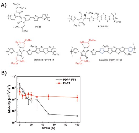
Inspired by the previously mentioned understanding, we have focused on Donor-Acceptor (D-A) type polymers, which are known to aggregate and possess excellent charge-carrier mobility. We demonstrated using an internally developed soft contact lamination method that PiI-2T has comparable mechanical properties as P3HT but a higher μFET of 1.52 × 10⁻² cm2V–1s–1 at 100% strain shown in Figure 1B.14 Unfortunately, the PDPP-FT4 investigated showed poor stretchability despite superior charge transport.

Figure 1.A) Chemical Structures of PiI-2T, PDPP-FT4, branched-PDPPFT4 and branched-PDPP-TFT4T. B) μFET of PDPP-FT4 and PiI-2T measured by soft-contact lamination method for various amounts of strain applied. Adapted with permission. Copyright 2014 American Chemistry Society.14
Back-bone and Side-chain Modification
To further account for the poor mechanical properties of PDPPFT4 and establish general design rules for stretchable D-A polymers, we considered two additional DPP-type polymers: branched-PDPP-FT4 with branched side-chains and branched- PDPP-TFT4T with branched side-chains and additional thiophene spacers between the fused tetrathienoacene as highlighted in Figure 1A.15 By measuring the tensile modulus and fabricating OFET from stretched polymer films we observed a decrease in modulus and an increase in ductility when incorporating branched side-chains. Furthermore, upon the addition of thiophene spacers, the polymer film did not show crack propagation until 40% strain and maintained a hole mobility of 0.1 cm2V–1s–1 up to 100% strain. This was attributed to the decrease in crystallinity and the entangled nonfibrillar texture observed by grazing-incidence X-ray diffraction (GIXD) and atomic force microscopy (AFM). With careful backbone and sidechain engineering we could manipulate a polymer’s molecular packing and backbone rigidity while maintaining good charge transport.
Stress Dissipation and Healing Mechanism through Hydrogen Bonding
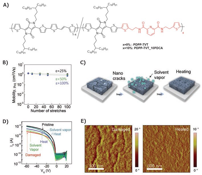
Introducing an energy dissipating mechanism is another effective strategy to impart stretchability.16 Following our previous work that displayed a highly stretchable and self-healing elastomer,17 we incorporated a 2,6-pyridine dicarboxamide (PDCA) unit with moderate hydrogen bonding (H-bonding) strength to a DPP polymer to give PDPP-TVT-10PDCA shown in Figure 2A.18 Compared to the control polymer PDPP-TVT, the PDCA polymer displayed a decrease in tensile modulus and an increase in fracture strain at 120% strain. Transistors prepared from strained polymer films gave a stable μFET above 1.0 cm2V–1s–1 up to 100% strain. Figure 2B shows the high durability of the polymer active layer which only showed a 26% decrease in μFET after 100 cycles of rigorous stretching at 100% strain. This improvement in toughness was attributed to the weak H-bonding from the PDCA unit which acts as a sacrificial bond and breaks upon strain, hence releasing stress experienced by the polymer chains.
Additionally, the dynamic nature of the H-bonding allowed the PDPP-TVT-10PDCA film to heal upon solvent and thermal annealing. Figure 2E shows the AFM images of the damaged film after stretching and the recovered film after solvent and thermal annealing. Clear nanocracks were observed initially, but after the healing treatment, cracks were no longer apparent and the μFET recovered back to above 1.0 cm2V–1s–1. This is the first demonstration of a semiconducting polymer with healing capability.

Figure 2.A) Chemical structures of PDPP-TVT and PDPP-TVT-10PDCA. B) μFET of PDPP-TVT-10PDCA versus number of stretching cycles performed perpendicular to strain direction in bottom-gate-top-contact device configuration. C) Schematic representation of the treatments used for healing the conjugated polymer films. D) Transfer curves of damaged and healed PDPP-TVT-10PDCA OFET. E) AFM phase image for damaged and healed film of PDPP-TVT-10PDCA. Reproduced with permission. Copyright 2016, Nature Publishing Group.18
Post-polymerization Modifications
Aside from modifying monomer structures, there are numerous post-polymerization modifications that can alter a material’s intrinsic mechanical properties, such as adding plasticizers, physical blending, crosslinking, hydrogenation, etc. While these techniques have been used for decades, very few have been tested with conjugated polymers. The advantage of postpolymerization modifications is their applicability to a variety of polymer semiconductors. This gives us an opportunity to convert brittle materials with good μFET to stretchable materials.
Crosslinking with Oligo-siloxanes
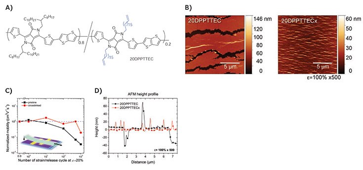
Decreasing backbone rigidity and increasing amorphous regions yields softer semiconductors with enhanced ductility. However, to improve the elasticity and fatigue resistance of a material, some form of crosslinking is required to prevent irreversible deformation upon strain. To test this, we crosslinked a DPP random co-polymer containing 20% crosslinkable side-chains (20DPPTTEC) with a PDMS oligomer to give 20DPPTTECx.19 The crosslinked film showed an increase in yield strain from 8% to 14% strain as determined by the buckling onset strain. More importantly, no cracks were observed even after 500 cycles of 100% strain. Figure 3D shows the height profile of the strained polymer film; 40 nm deep cracks and 60 nm tall wrinkles were formed in the pristine film, whereas 20 nm tall wrinkles were found in the crosslinked film, highlighting the improved elasticity. To assess the fatigue resistance of the polymer films, they were subjected to cyclic loading of 20% strain. The pristine polymer started showing decay in μFET after 10 cycles of 20% strain whereas the crosslinked films maintained a μFET of 0.4 cm2V–1s–1 up to 500 cycles. Interestingly, the siloxane crosslinkers also showed a plasticizing effect, which accounted for a decrease in tensile modulus and crystallinity as observed by GIXD.

Figure 3.A) Chemical structure of 20DPPTTEC. B) AFM height image of 20DPPTTEC and 20DPPTTECx relaxed from 500 cycles of 100% strain. C) Normalized μFET of 20DPPTTEC and 20DPPTTECx versus number of stretching cycles at 20% strain performed perpendicular to strain direction. D) AFM height profile of 20DPPTTEC and 20DPPTTECx after 500 cycles of 100% strain. The crosslinked polymer forms 20 nm tall wrinkles upon cyclic loading, whereas the pristine polymer forms microcracks and 60 nm tall wrinkles. Reproduced with permission. Copyright 2016 Wiley-VCH.19
Nanoconfinement through Blending with SEBS Polymer
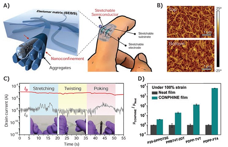
While nanoconfinement is a known strategy to alter a polymer’s ductility, chain dynamics, and modulus, it had never been previously studied using conjugated polymers. By blending conjugated polymer DPPT-TT (Cat. No. 791989) with 70 weight % of SEBS, we obtained polymer films that showed vast improvement in mechanical properties while maintaining excellent electrical properties.20 The comparable surface energies of the semiconductor and elastomer leads to a nanoscale phase-separation upon blending as shown in Figure 4B. The confinement effect from the SEBS matrix suppresses crystallization in the film and decreases the glass transition temperature of the polymer, which leads to a decrease in modulus and increase in fracture and yield strain. The blended film could be stretched to 100% strain with no cracks and no apparent decrease in μFET. To date, almost all stretchable polymer active layers show compromise in μFET when compared to their parent polymer. However, our SEBS-polymer blend showed no degradation in electrical properties when compared with the pristine DPPT-TT semiconductor. This is due to the strong aggregation that is maintained in the polymer blend despite a decrease in crystallinity. Furthermore, the SEBS could impart elastic properties to the polymer film, showing stable μFET up to 1,000 cycles of 25% strain. Figure 4C shows the drain current from the fully stretchable transistor under stretching, twisting, and poking by sharp object. The stable drain current demonstrates the robustness of the device prepared from the polymer blend. Finally, the general applicability of this method was tested with various conjugated polymers. Of the additional four polymer semiconductors tested, three could achieve μFET above 1.0 cm2V–1s–1 under 100% strain and none of the polymers displayed cracks under optical microscopy. Figure 4D shows the improvement in mobility of each polymer under nanoconfinement at 100% strain. Even the brittle PDPP-FT4 discussed earlier showed uniform films under strain and four orders of magnitude

Figure 4.A) A 3D schematic of the desired morphology composed of embedded nanoscale networks of polymer semiconductor, which can be used to construct a highly stretchable and wearable OFET. B) AFM phase images of the top and bottom interface of the nanoconfined film with 70 wt % SEBS and 30 wt % DPPT-TT. C) Drain current (ID) and gate current (IG) of a fully stretchable transistor under sequential stretching, twisting, and poking with a sharp object. D) Normalized μFET of neat films (gray) and the corresponding blended film of these conjugated polymer, under 100% strain. Reproduced with permission. Copyright 2017 AAAS.19
Conclusions
In this article, we have summarized five different strategies for developing intrinsically stretchable polymer semiconductors for OFET. This includes utilizing the high μFET and aggregating properties of D-A polymers, side-chain and backbone engineering, the addition of H-bonding moieties, covalent crosslinking, and the introduction of nanoconfinement via SEBS blends. These approaches have successfully allowed us to decrease polymer rigidity and crystallinity, resulting in softer and more ductile films. Film toughness and elasticity were also greatly improved, giving greater fracture strains and fatigue resistance. H-bonding units further allowed films to heal from nanocracks upon solvent and thermal annealing. Soft, healable, robust, and intrinsically stretchable transistors are essential steps towards the development of implantable devices as well as next generation bioelectronics.
Materials
References
To continue reading please sign in or create an account.
Don't Have An Account?