CoMoCAT® Single-wall Carbon Nanotubes
Single-wall Carbon Nanotubes: Recent Advances, Manufacturing, Characterization and Applications
Section Overview
Introduction
Carbon nanotubes are materials that possess remarkable properties which find utility in a wide range of new and enhanced applications in printed electronics, sensors, flexible displays, e-readers, medical treatment, energy storage and more. Since their discovery in 1991 by Ijima, SWNTs have stimulated a great deal of activity in both the global research community and industry, and have inspired much investment in manufacturing methods, characterization and application development. Here we briefly describe the physico-chemical nature and characterization of single-wall carbon nanotubes (SWNTs) and the status of their commercialization. Multi-wall carbon nanotubes (MWNTs) are discussed separately in our MWNT Spotlight.
Structure of Carbon Nanotubes
SWNTs are an allotrope of sp hybridized carbon similar to fullerenes. The structure can be considered as a cylindrical tube comprised of 6-membered carbon rings, as in graphite. The cylindrical tubes may have one or both ends capped with a hemisphere of the buckyball or fullerene structure.
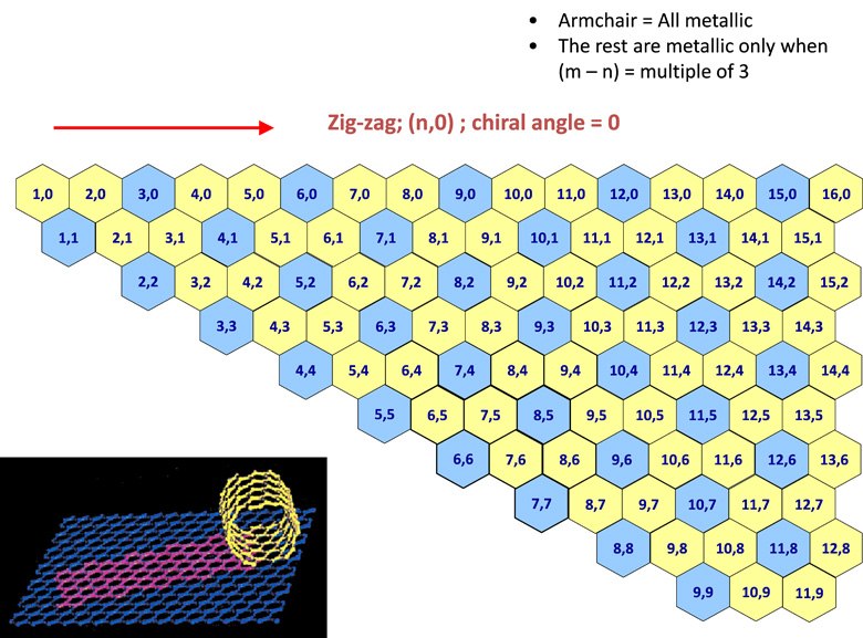
An understanding of SWNT structure requires familiarity with the concept of nanotube chirality, since the chirality of a SWNT dictates many of its properties. The chirality map, illustrated in Figure 1, has been developed as a tool for understanding chirality and its implications.

Figure 1.A chirality map which shows the various types of SWNTs that can be formed. The properties are governed by the way in which they are rolled as shown in the inset. The SWNT will be metallic in the armchair configuration, or when m-n is a multiple of 3.
A SWNT can be envisioned as a sheet of graphene one atom thick rolled into a tube (inset in Figure 1). The chirality describes both the orientation and diameter to which the sheet is rolled. Each SWNT on the chirality map is defined by two integers, (n,m). Chirality defines many of the properties of the individual SWNT. For example, SWNT shown on the chirality map in blue are metallic in nature. These are tubes where n=m (armchair) or n – m = 3i, (where i is any integer). Those depicted in yellow are semiconducting, displaying different band gaps depending on the length of the chiral vector.
Unique Properties of SWNT
Mechanical: Individual SWNTs are significantly stronger than steel. Calculated values for tensile strength of SWNT are ~ 100 times greater than steel at 1/16th the weight. The highest measured value is approximately half of the predicted theoretical strength, the difference possibly being due to defects in the structure.
Electrical: Individual SWNTs have current carrying capacities of 109 amp.cm-2, higher than those of copper or gold, and semiconducting species exhibit higher electron mobility than silicon.
Optical: SWNTs have a distinct optical absorption and fluorescence response, with each chirality demonstrating its own characteristic absorption and fluorescence spectrum.
Thermal: Room temperature thermal conductivity of a single nanotube may be comparable to that of diamond or in-plane graphite, which is generally thought to display the highest measured thermal conductivity of any known material at moderate temperatures.
Challenges of SWNTs
Technical hurdles in the areas of purity, selectivity and dispersibility have so far limited the widespread application of SWNTs. However, much recent progress has been made to address each of these obstacles.
Purity: The various manufacturing processes used in the production of SWNTs lead to products which are contaminated to varying degrees with residual catalyst and other forms of carbon. For many applications, further purification processes are necessary to remove these contaminants to provide product of sufficient purity. More recently, methods of synthesis that minimize the 'synthesized' impurities have become commercially available.
Selectivity: As described above, the SWNTs are a mixture of tubes of different chiralities, some of which are electrically conducting and some are semiconducting. It is desirable for many applications to isolate the types of tubes from one another, such as metallic from semiconducting and for some applications, tubes with well-defined individual chirality. Laboratory scale methods to achieve a very high degree of selectivity have been reported, and efforts to develop scalable separation processes are bearing fruit. Manufacturing processes such as the CoMoCAT® catalytic CVD process have been shown to provide a high degree of selectivity toward certain chiralities in SWNTs as synthesized, making the yield of secondary purification processes substantially higher or even unnecessary.
Dispersibility: SWNTs can be difficult to disperse, partly because of their well-known tendency to form ropes or bundles due to Van der Waals attraction between the tubes. However, they can be dispersed in aqueous solutions with the aid of suitable surfactants either as small bundles or as individual tubes, or at low concentrations with appropriate functionalization. Exfoliation of bundles can be achieved by sonication of aqueous solutions of SWNTs in the presence of surface active molecules such as DNA, sodium deoxycholate and sodium cholate. To quantify the degree of nanotube exfoliation obtained in a given dispersion, Tan and Resasco defined the concept of resonance ratio from the optical absorbance spectrum. The area of the resonant band divided by the area of the non-resonant background in this ratio allows easy comparison of results independent of the absolute absorption. Dispersants could then be ranked for their effectiveness using this parameter.
Additionally, dispersion of SWNTs in resins and thermoplastics is limited by a dramatic build up in viscosity caused by the entanglement of the SWNTs bundles. Various proprietary methods exist to circumvent this problem, and new hybrid forms of SWNTs are being developed to address this issue.
Synthesis of SWNTs
Various methods have been used in the manufacture of SWNTs. These include laser ablation, carbon arc and CVD processes, either involving a gaseous catalyst as in the HIPCO® process or using a supported catalyst as in the CoMoCAT® process. The laser ablation process is used primarily for research materials. The carbon arc process produces long tubes with diameters in the range 1.4 to 2.0nm, but carbon arc material has a large amount of impurities and for most applications will require extensive purification. The CVD processes offer the best approach to the manufacture of larger SWNTs quantities, with perhaps the most scalable being the CoMoCAT® process which uses a fluidized bed reactor similar to those used in petroleum refining, albeit, currently on a much smaller scale. The supported catalyst approach also offers the unique ability to provide a substantial degree of chirality control during synthesis.
Characterization of SWNTs and Quality Assurance Parameters
As discussed above, the properties of carbon nanotubes vary with the individual SWNT chirality. Since at this time all SWNTs are produced as a mixture of chiralities, the properties of the material will depend on the proportions of chiralities present. Many analytical techniques have been deployed to determine the structure of SWNT materials. These range from observational techniques such as SEM, TEM, AFM and STM to spectroscopic techniques such as UV-Vis-NIR, photoluminescence (PL) and Raman. In addition to these methods, X-ray diffraction has been used by Miyata et al. to confirm the chirality assignments in the optical spectrum of SWNTs. Thermogravimetric analysis (TGA) has been used extensively to determine the onset of oxidation, maximum oxidation rate and the mass of catalyst retained in the product. In some cases, it is possible to obtain a reasonable estimate of purity from the TGA curve.
TEM and SEM have been widely used to assess SWNT purity. However, these are unreliable for any quantitative estimation of purity. A typical TEM or SEM image uses ~ 1pg of material over an area of 1 to 4 μm2 and it would therefore take the analysis of many micrographs imaged randomly throughout a macroscopic sample to obtain any meaningful results of the overall purity. Furthermore, there are no suitable algorithms for objectively determining the relative proportions of the different species seen in typical unpurified SWNT material. Thus, while TEM and SEM can give good information on the structure of the product, they must be used with caution and considered only as qualitative indicators of purity.
There are three relatively straightforward and commonly available techniques that can be used in combination to ensure that consistent high quality SWNTs are produced. For quality assurance purposes, Raman spectrum can be used as a rough purity fingerprint. TGA provides a measure of residual catalyst and, as will be discussed further below, a reasonable measure of the SWNTs content. Optical absorption measurements in the UV-Vis-NIR region can be used to ensure consistent chirality control.
Raman spectroscopy
Analysis by Raman spectroscopy has been widely used for determining both the detailed combination of chiralities present in the SWNTs material and for assessing purity. There are three areas of the Raman spectrum of primary interest for SWNTs. The radial breath mode (RBM) from approximately 120 to 300 cm-1 is unique to SWNTs and can be used to determine tube diameter from the equation:

where, d is the SWNT’s diameter in nm and ν is the wave number in cm-1.
It is important to note that to get a complete picture of the chiralities, several lasers of different excitation frequency must be used. Using a continuously variable laser to excite the SWNTs, Jorio, et al. have mapped the chiral structure of SWeNT® SG65 (Product No. 704148).
There are two additional bands seen in the Raman spectrum of SWNTs: the D band at ~ 1350 cm-1 is indicative of disordered carbon, multiwall tubes and microcrystalline graphite, and the G band at 1500 to 1586 cm-1 is a result of the tangential stretching mode from graphitic-like materials. The ratio of the height of the G band to that of the D band has been widely used as a measure of the purity of SWNTs. However, caution must be used when measuring this ratio as the G band is a resonant band and is therefore much stronger than the D band. It is probably best to say that a high G:D ratio is a necessary condition for high purity SWNTs, but it is an insufficient assurance of purity since other methods must be used in conjunction with this parameter. For example, other forms of graphitic carbon may contribute to a strong G band.

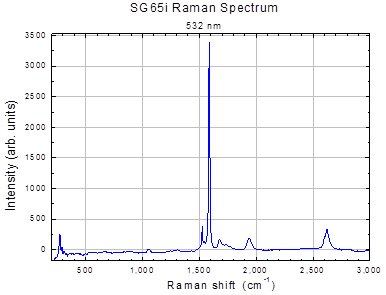
Figure 2.Ramen spectrum of SWeNT® SG65i SWNT (Product No. 773735)
The Raman G:D ratio, with the cautions listed above can be used as a first measure of purity. A typical Raman Spectrum for SWeNT® SG65i (Product No. 773735) is shown in Figure 2.
Optical Absorption
Optical absorption (OA) measurements in the UV-Vis-NIR region show characteristic peaks of individual (n,m) species superimposed on the π-plasmon background. For example, the (6,5) species absorb at 566 and 976 nm and in response fluoresce at 983 nm. A (7, 6) absorbs at 645 and 1024 nm and fluoresces in response at 1030 nm. These individual peaks have been used as a basis for estimating the purity of SWNTs. Nair, et al. have developed a method for computing the baseline for the spectrum, which then a calculation of peak heights and areas for the individual (n,m) species. For simplicity, we usually transform the measured OA spectrum to the energy domain, where the background becomes linear in the area of interest for SWNT characterization. Figure 3 shows a typical OA spectrum for SWeNT® SG65i material. The inset shows the spectrum in the more conventional form with the absorption plotted as a function of wavelength. Measurements of the height of the strongest peak (P2B), and integration of the overall signal (S2B) can be used to ensure that the product is consistent. We primarily use P2B as a control parameter for SWeNT® SG65i (Product Nos. 773735) and SG76 (704121) nanotubes where one particular tube type is dominant. P2B is defined as the height of the highest peak in the spectrum between 350 and 1,350 nm divided by the background at that wavelength.
P2B= Height of (6,5) or (7,6) Signal Peak
Height of Background Peak

Figure 3.Optical absorbance spectrum in the region of UV-Vis-NIR of SWeNT® SG65i (Product No. 773735)
It should be noted that the OA methodology as described here uses the OA spectrum measured after dispersing and centrifuging the SWNTs sample. It is used as a measure of chirality control rather than overall purity. Measurement of the absorbance at a particular wavelength before and after centrifugation gives a measure of the dispersibility of the SWNTs.
Thermogravimetric Analysis (TGA)
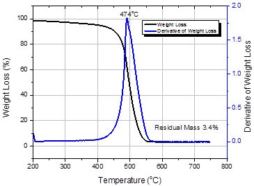
A typical TGA curve for SG65i SWNTs is shown in Figure 4. TGA is used to assess the purity of the material. The primary quality parameters determined from the TGA analysis is the residual mass at 625 °C. This is a measure of the residual catalyst metals (now oxidized) retained in the material. A second peak in the derivative curve has been attributed to the presence of other forms of graphitic carbon that oxidize at higher temperatures than SWNT. With improvements in both the catalyst manufacture and SWNT synthesis other forms of carbon have been reduced to such a low level that they are no longer measureable by TGA. The residual mass is expressed as a percentage normalized for the weight loss at 200 °C.
Residual Mass = Weight Loss at 625 °C
Initial Weight Loss

Figure 4.Thermogravimetric analysis of SWeNT® SG65i (Product No. 773735)
Combined, these three methods give a good measure of purity and consistency of the SWNTs. However, as SWNT applications are developed further, functional testing, such as electrical conductivity measurements, will be needed to link the purity data to SWNTs performance.
Applications of SWNTs
The numerous unique properties of SWNTs have led to extensive research to develop its use in a wide range of applications. Their highly conductive nature and large surface areas are utilized to prepare conductive polymer composites and films, improved lithium ion batteries, and supercapacitors. Optical properties allow for their use as electrodes in displays, solar cells, and emerging solid state lighting technologies. The semiconducting nature of some SWNTs species allows their adaptation to logic devices, non-volatile memory elements, sensors and security tags.
Most CNT manufacturing methods produce a highly poly-disperse product – a wide range of diameters and chiralities, compromising optical, electrical and chemical properties. Many SWNTs synthesis methods produce a significant amount of other forms of carbon and metal and metal oxides which in the majority of cases need to be removed using expensive secondary processing. Chiral separation methods, post-synthesis, are very expensive and have low yield, starting with materials generally containing about 66% semiconducting species and 33% metallic species. High manufacturing costs and limited capacity resulting from the above have stifled market acceptance.
However, recent developments by Southwest Nanotechnologies (SWeNT®) have successfully addressed each of these problems with a new product called SG65i (Product No. 773735). SG65i represents an improvement over SG65, the material that is the starting material for NIST’s (National Institute of Standards and Technology) Standard Reference Material, and was until recently the most chirality-selective of available materials as synthesized. A comparison of the two materials is here is
Table 1.
Both materials are made using the patented CoMoCAT® synthesis process, well known to be more selective for chirality and diameter than alternative methods. Significant improvement of the catalyst system in SG65i has further improved selectivity. These enhanced properties are enabling accelerated development of printed semiconductor devices, notably thin film transistors (TFTs). TFTs require a high concentration of semiconducting SWNT to achieve the On/Off ratio and mobility needed at the low cost required for widespread acceptance of OLED TV, for example. SG65i will allow high yields of the 99%+ semiconducting material required, whereas other commercially available SWNTs typically have only the ‘natural’ proportion of semiconducting species, 67%. But starting with a low initial concentration of semiconducting species and a wide distribution of diameters and chiralities, the yielded cost of such materials can be prohibitive for commercial applications. At ≥ 95% semiconducting SWNTs concentration, the task of purifying to the required level is much simplified.
This performance, and the high degree of flexibility and 'stretchability' inherent to SWNT coatings will also enable printed, flexible semiconductors for flexible electronics, a range of applications long pursued but not yet a commercial reality.
Another exciting application area for SWNTs, and especially for SWeNT®, is in the medical arena, perhaps most notably in cancer treatment. Several promising research projects are underway which depend on a high concentration of tubes of the (6,5) chirality, or other similar small diameter species. These projects take advantage of the unique optical properties of tubes of this chirality – when irradiated with light in the near-infrared (NIR) region these SWNT fluoresce in the infrared, resulting in the ability to heat internal tissue in the area of the cancer by irradiation of SWNT placed in the area of the malignant tissue. In this case the high concentration of (6,5) SWNT in SG65i are expected to make preparation of materials much more practical.
For transparent conductive films (TCFs), SWNT are beginning to be adopted as replacements for ITO and conductive polymers such as PEDOT:PSS (Product Nos. 768642 and 739316). Many applications of TCFs have optoelectronic properties beyond the range of current SWNT-based coatings, but a wide range of applications are well within the ‘window’ of SWNT capability. In these cases, a limitation was customer confidence in the availability of a sufficiently consistent product, a scalable manufacturing method to support emerging applications, and a product that provides good optoelectronic performance. To meet these requirements, SWeNT® has developed its most conductive grade CG300 (Product No. 775533), made by CoMoCAT®, widely recognized for its scalability and the consistent product it produces, with tailored characteristics that make it particularly suited for inclusion in the inks needed for printing and coating.
Conclusion
Despite early excitement about SWNTs materials and the extraordinary amount of research inspired by their discovery, to date commercial exploitation of the technology has been limited. However, momentum is now building, driven by substantial recent progress in several fundamental areas. We can expect to see a dramatic expansion of applications as the barriers are now being overcome.
Listed below are CoMoCAT® high purity SWNTs manufactured by SouthWest NanoTechnologies (SWeNT®), Inc. and available in research quantities exclusively from Sigma-Aldrich Materials Science.
References
如要继续阅读,请登录或创建帐户。
暂无帐户?