Atomic Layer Deposition (ALD)
Introduction
Although the process was developed during the 1970s, atomic layer deposition (ALD) remained more of a niche process, since initially most applications of this technique were bound to electronics. In recent years considerable interest in ALD has emerged, mainly due to its ability to controllably coat even very small structures, e.g. nanoor microstructures. Using various strategies and modifications, a number of groups worldwide have produced novel structures or functionalized materials. Some of the most innovative and promising strategies include template-directed synthesis of novel structures, area-selective deposition of materials, low-temperature ALD deposition temperature-sensitive subtrates, and the development of new processes to increase the versatility of ALD.
All of these applications of ALD show the power of this deposition method and its impact on advanced materials research. Particularly simple yet effective processes together with the increasing number of commercially available ALD reactors have attracted the interest of scientists worldwide as reflected in the increasing number of scientific publications in the field of “nano-ALD.”
In this manuscript a few examples of work, including the above-mentioned areas, will be shown. A more comprehensive review can be found elsewhere.1
The ALD Process
The ALD process is a vapor-phase, thin-film deposition method chemically similar to chemical vapor deposition (CVD). The similarity can be seen from the fact that ALD precursor materials can be used for CVD, however, not necessarily vice versa. Physically, there are significant differences. Using the example of Al2O3-deposition from trimethylaluminum (TMA, Product No. 663301) and water. The major difference between CVD and ALD will be explained.
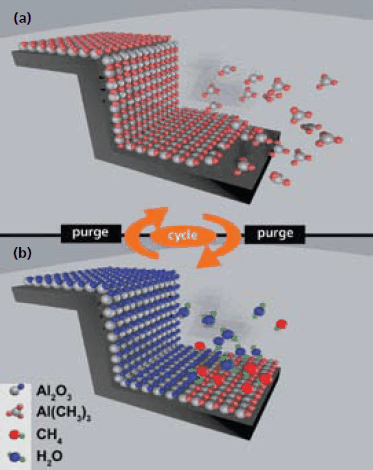
While in the CVD process two precursor materials, TMA and H2O, are jointly introduced into a reaction chamber to produce Al2O3 which deposits on a substrate, in the ALD process the chemical reaction is split into two half-reactions. Initially the substrate is exposed to TMA forming a chemisorbed (sub) monolayer (Figure 1a). After adsorption the excess TMA in the gas phase is removed by purging. Successively the substrate is exposed to H2O to react with the (sub)monolayer of TMA forming a layer of Al2O3 (Figure 1b). Removal of the reaction products (here: methane) and excess of H2O finishes one cycle of growth, which can be repeated until the desired thickness of the layer is obtained. If the process is performed in a precursorspecific temperature range, the so-called “ALD-window,” the growth of the film is linear and the thickness can be controlled on the Å-scale.

Figure 1. Schematic of one cycle of an ALD process. The schematic illustrates a simplified model for the deposition of Al2O3 using TMA and water as precursors.
The big advantage of ALD is that the process is driven by the chemical saturation of surfaces with the precursor (e.g., TMA) rather than a directed deposition, as is the case with CVD. Therefore the ALD process allows for conformally coatings of surfaces of nanopores even with very high aspect ratios2 or very complex materials such as aerogels.3
Template-Directed Synthesis of Nanostructures
Template-directed synthesis of nanostructures is the fastest growing area in ALD. Various templates can be used for conformal coating and replication or functionalization of nanostructures. These include nano- and microporous substrates, arrangements of nanospheres, nanowires, nanotubes or even single nanoparticles.
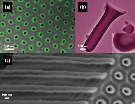
Probably, the easiest method for templated nanostructure synthesis involves the use of porous materials. During the past few years a number of manuscripts have been published, showing the synthesis of nanotubes from a variety of materials or even arrays of nanotubes.2 More recently, the focus of nanotube synthesis has shifted from the deposition of basic materials towards functional materials. Recently, for example, the ability to produce magnetic nanotubes from nanoporous anodic alumina templates by ALD deposition of iron oxide (Figure 2) or nickel has been shown.4,5

Figure 2. Electron micrographs (scanning, SEM; transmission, TEM) of iron oxide tubes. Scale bars: 100 nm. (a) SEM of an array of narrow tubes (11±4 nm Fe2O3, green circles) embedded in the alumina template; contrast enhanced by colorization. (b) TEM of a single thick and short tube (42±4 nm Fe3O4) isolated by dissolution of the template; the inset zooms in on the very smooth wall. (c) SEM of an array of thick ZrO2/Fe2O3/ZrO2 tubes (12±2/26±4/12±2 nm) embedded in the template: edge view at a crack, with tubes broken in their length and emerging on the top side of the membrane. Image reprinted with permission from J. Am. Chem. Soc. 2007, 129, 9554–9555, Copyright 2007 American Chemical Society.
Similar to nanoporous materials, nanowires can also be used as templates for ALD deposition on and successive removal of the initial nanowire. Inducing a solid-state diffusion reaction also produces nanotubes in specific circumstances.6,7
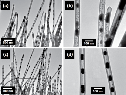
A trend towards the synthesis of functional nanostructures has been observed. Recently, a combination of ALD deposition, reduction and initiation of the Rayleigh instability led to the synthesis of TiO2-nanotubes with incorporated Cu-nanoparticles in a regular nanochain arrangement (Figure 3).8 After optimization such nanostructures may find future application in nanooptics or plasmonics.

Figure 3. TEM images of Cu nanoparticle chains prepared by reduction of CuO nanowires with 20 nm Al2O3 shells with H2 for 1 h at different temperatures: (a,b) sample prepared at 600 °C; (c,d) sample prepared at 750 °C. Panels (b) and (d) are TEM images corresponding to panels (a) and (c) at higher magnification. Image reprinted with permission from Nano Lett. 2008, 8, 114–118. Copyright 2008 American Chemical Society.
Advanced optical nanostructures produced by ALD already exist. Due to the benefits of this deposition method the production of inverse opal structures from a variety of materials by replicating highly ordered arrangements of nanospheres became possible. Research groups at Georgia Institute of Technology and Harvard University have been very active in this field. A number of various inverse opals were synthesized by ALD and characterized. The materials deposited include WN, TiO2, Ta3N5, ZnO, GaAs or even TiO2/ZnS multilayers.9–12 Such structures show enormous potential, for example, as photonic crystals. Thanks to this simple synthesis method such structures can and surely will be further developed in the coming years.
A comparatively difficult area is the use of carbon nanotubes (CNTs) as templates. As the surface of carbon nanotubes is rather inert, it becomes very difficult to coat CNTs by ALD. Nevertheless, due to their shape and stability CNTs remain very interesting as templates. Therefore strategies were developed in order to achieve uniform coatings. Various reports showed that after functionalization of CNT with, for example, NO2, a coating with Al2O3, HfO2 or Ru-oxide indeed becomes possible.13–16 These coatings could be beneficial for the improvement of the physical and/or chemical properties of the CNT. However, technological use will still require further research and development.
Probably the most difficult nanoscale template for ALD is a single nanoparticle. Although it might be easily coated, difficulties in handling such materials appear frequently. If one wants to obtain a continuous conformal coating, one has to prevent any contact of the nanoparticles with each other and/or with the walls of the reactor. Nevertheless, here too some progress has been achieved. A group in Boulder, Colorado, showed that there are at least two ways to handle nanoparticles during ALD deposition in order to obtain conformality.17
Area-Selective Deposition of Materials
A highly interesting field of development in ALD is area-selective deposition. Although the most powerful application of ALD is the conformal coating of all accessible surfaces, there is the possibility to direct the deposition to discrete areas by chemically tuning them. Patterns of lithographically produced structures can be selectively switched to hydrophilic or hydrophobic (e.g., by various silanes) in order to direct or prevent the adsorption of precursor molecules.18 This route is a very elegant way to obtain nanoscale patterns of materials needed for certain applications. The principle itself is simple as well as effective. Most likely this strategy will be broadly applied to deposit a variety of materials in a structured manner in order to obtain electronically or optically active materials.
Low-Temperature ALD Deposition
Low-temperature ALD (LT-ALD) is playing an increasingly important role. In thin film deposition the ability to coat materials that are temperature-sensitive and cannot be coated with other methods (e.g. CVD); substrates include polymers or biological templates.
Initial experiments on LT-ALD were performed in 1994, involving deposition of SiO2 at room temperature.19 Since then a number of (LT-ALD) processes were successfully developed for materials like CdS, Al2O3, TiO2, B2O3, V2O5, HfO2, ZrO2, ZnO and even metallic Pd.1, 20, 21 Although this list of materials is already impressive, undoubtedly a larger number of available processes, particularly for the deposition of metals would be of high interest. If one considers the possibility to deposit metallic electrodes on polymer structures in order to obtain flexible electrodes, the significance of LT-ALD becomes obvious. Development in this area is at the very beginning and one can expect that more materials will be deposited by LT-ALD technique in the near future.
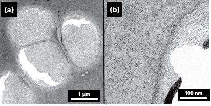
A particularly interesting application of LT-ALD is the possibility to coat or functionalize biological nanostructures. Nature has already applied nanotechnology for millions of years. If one considers the hydrophobicity of lotus leaves, which is related to micro- and nanostructures, it becomes obvious that mankind can still learn from nature. In some cases nature provides perfect nanostructures, which could easily be replicated thus avoiding more complex growth and fabrication with nanometer precision. However, one of the limiting factors here is the technology involved; for example, in the case of ALD the vacuum process and the deposition temperature. As the vacuum process cannot be avoided, for structures that are vacuum resistant, the deposition temperature is of significance. A few attempts have already been reported to coat biological nanoand microstructures by ALD. Initial experiments of this kind involved the coating of plant viruses and ferritin spheres with metal oxides, which lead to tiny metal oxide nanotubes and freestanding films with embedded ferritin molecules (Figure 4).

Figure 4. TEM (200 kV) images of ferritin molecules treated with Al2O3(a) and TiO2(b) by ALD. The images show ferritin molecules embedded in amorphous freestanding Al2O3 and TiO2 films. The darker gray areas originate from the holes in the carbon film on the TEM grid. The black spots in image (b) show the iron oxide core of ferritin. The films have cracks, and on image (b) the free-standing film is rolled up from the side, which was caused by the electron beam from the TEM. Image reprinted with permission from Nano Lett. 2006, 6, 1172–1177. Copyright 2006 American Chemical Society.
Further work showed the possibility to coat nanostructured butterfly wings with Al2O3 and thus to obtain structured samples with various colors that depend on the thickness of the coating.22 Although this field is emerging slowly, it is expected that there will be much more activity and progress in the near future.
Novel Processes
Since the development of ALD, much of the work was dedicated to the development of new processes. A large number of materials, mainly metal-oxides, but also nitrides, carbides, sulfides, phosphides and metals have been successfully deposited. The known instances cover a major part of the Periodic Table either as pure elements or as binary or ternary compounds.
While most of the developed processes concentrated on materials, which in one way or another are interesting for electronic or optical applications, there are also other important areas of application. A particularly attractive new process, the deposition of apatite by ALD, may find broad application in the synthesis of biocompatible materials.23 There will be a large number of possible applications if such processes can be applied routinely and in a controlled manner.
Another highly interesting novel group of materials deposited by ALD are polymers or their derivatives. In 1991, the principle of polymer-ALD, the so-called molecular layer deposition (MLD) was demonstrated.24 However, not much attention was paid to this work until about 15 years later when new attempts were made to produce very thin polymer films. Since then the ALD process has become a really versatile tool for thin film deposition, as not only inorganic materials can be deposited, but also organic molecules. Moreover, studies on the synthesis of hybrid materials of organic and inorganic molecules stacked in a layer-by-layer manner were performed. More insight into this particular field of ALD (MLD) is given in the article on page 34 by S.M. George et al. in this issue of Material Matters.
Further development in this direction will be of high interest, since hybrid organic-inorganic materials may exhibit unique properties and prove useful for a variety of biomedical or environmental applications.
Conclusion
ALD has emerged as the method of choice for the controlled and conformal deposition of thin layers involving micro- or nanostructures. A large number of materials can be deposited by ALD. The possibility of obtaining a reactor commercially as well as the steadily increasing number of precursors make the ALD process especially convenient and attractive for newcomers to this field. Even though there are still limitations in particular processes or precursors for very special purposes, in general, the only limitation to further applications of ALD appears to be the imagination and creativity of the researchers involved.
Acknowledgment
Dr. Mato Knez gratefully acknowledges financial support by the German Ministry of Education and Research (BMBF) under the contract number 03X5507.
To continue reading please sign in or create an account.
Don't Have An Account?