
form
dispersion
concentration
2.5 wt. % in 2-propanol
particle size
<50 nm (BET)
density
0.7992 g/mL at 25 °C
Quality Level
General description
该WO3-x 纳米粒子墨水可用于狭缝染料,旋转涂布和刮刀涂布,从而用作印刷电子器件中的空穴传输层。氧化钨纳米颗粒墨水是基于氧化钨(WO3)纳米颗粒在异丙醇中的胶体悬浮液的一种孔选择性界面层墨水。WO3颗粒的平均大小已优化为12-16nm左右。氧化钨纳米颗粒在亲水性和疏水性基体上具有较高的加工性能和易成层性。WO3-x 纳米粒子墨水普遍适用于普通和倒置结构的太阳能电池。
退火温度<100°C。
退火温度<100°C。
Application
WO3 纳米粒子墨水可以作为空穴提取层(HEL)材料应用于OPV电池中。氧化钨纳米粒子墨水可与PEDOT:PSS配方混合,以微调电子和形态干层特性(例如导电性、表面粗糙度或层孔隙率)。
Other Notes
使用前:超声波和(可选)通过0.45 μm PTFE过滤器过滤
工作条件:在氮气(或低湿度)下使用和薄膜干燥
后处理:在80°C-120°C下对沉积的WO3-x 薄膜进行退火
工作条件:在氮气(或低湿度)下使用和薄膜干燥
后处理:在80°C-120°C下对沉积的WO3-x 薄膜进行退火
Legal Information
Avantama Ltd.的产品。
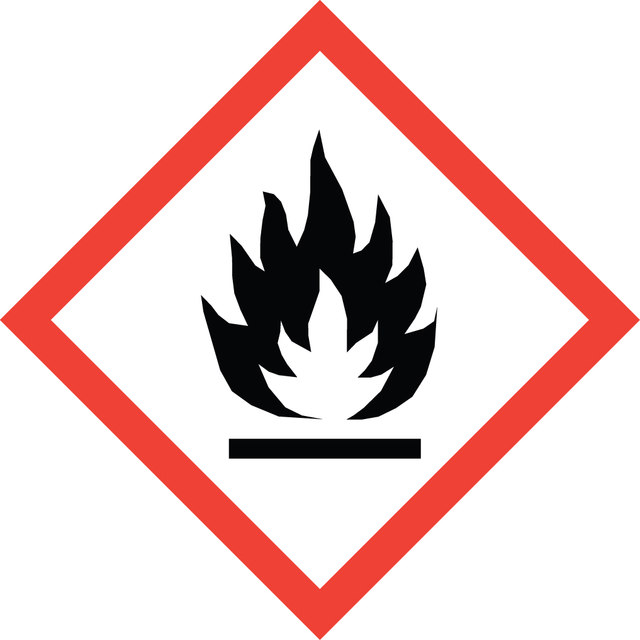

signalword
Danger
hcodes
Hazard Classifications
Eye Irrit. 2 - Flam. Liq. 2 - STOT SE 3
target_organs
Central nervous system
存储类别
3 - Flammable liquids
wgk
WGK 1
flash_point_f
53.6 °F - closed cup
flash_point_c
12 °C - closed cup
法规信息
危险化学品
此项目有
Inverted structure organic photovoltaic devices employing a low temperature solution processed WO3 anode buffer layer
Christoph J. Brabec; et al.
Organic Electronics, 13(11), 2479-2484 (2012)
High Fill Factor Polymer Solar Cells Incorporating a Low Temperature Solution Processed WO3 Hole Extraction Layer
Christoph J. Brabec; et al.
Advanced Energy Materials, 2, 1433-1438 (2012)
Lin Zhou et al.
Scientific reports, 9(1), 8778-8778 (2019-06-21)
This paper presents perovskite solar cells employed with WO3 nanoparticles embedded carbon top electrode. WO3 nanoparticles works as an inorganic hole-transport material (HTM) to promote the hole-extraction in the perovskite/carbon interface as revealed by efficiency, electrochemical impedance and external quantum
A universal method to form the equivalent ohmic contact for efficient solution-processed organic tandem solar cells
Journal of Material Chemistry A, 2, 14896?14902-14896?14902 (2014)
Flexible organic tandem solar modules with 6% efficiency: combining roll-to-roll compatible processing with high geometric fill factors
Energy & Environmental Science, 7, 3284?3290-3284?3290 (2014)
商品
Progress in solution-processed functional materials leads to thin-film optoelectronic devices for industrial and consumer electronics.
Professors Tokito and Takeda share design principles and optimization protocols for organic electronic devices, focusing on flexibility and low cost.
Find advantages of inorganic interface layer inks for organic electronic & other applications.
我们的科学家团队拥有各种研究领域经验,包括生命科学、材料科学、化学合成、色谱、分析及许多其他领域.
联系客户支持