Polymer-Sorted Semiconducting Carbon Nanotubes for Transistors and Solar Cells
Introduction
Single-walled carbon nanotubes (SWCNTs) are promising materials for use in the active channel of field-effect transistors (FETs), photoabsorbing layers of solar cells and photodetectors because of their ultrafast charge transport mobility,1 tunable near-infrared band gaps,2 and strong optical absorptivity.3 Substituting traditional semiconductors with semiconducting SWCNTs (s-SWCNTs) has the potential to pave the way for advances in a number of applications: high performance computation, high bandwidth and high efficiency wireless communications, wearable devices, and renewable energy.
One substantial challenge in developing these applications using SWCNTs is their electronic heterogeneity. As-synthesized SWCNTs contain a mixture of both metallic SWCNTs (m-SWCNTs) and s-SWCNTs at a ratio of 1:2. The presence of m-SWCNTs limits the performance of electronic and optoelectronic devices by creating electrical short-circuit pathways and rapidly quenching photoexcitations in nearby s-SWCNTs.
In the last decade there have been significant advances in the postsynthetic sorting and isolation of s-SWCNTs. This article highlights one of the most promising sorting systems, polyfluorene derivatives. This material is capable of isolating s-SWCNTs to purities greater than 99.9% and also sorting SWCNTs by their diameter and bandgap, both of which are determined by the (n,m) chirality of each SWCNT. We have exploited the exceptional electronic-type purity of s-SWCNTs that have been prepared using polyfluorenes in order to harness the extraordinary properties of s-SWCNTs in conventional transistors, in flexible and stretchable transistors, and in photovoltaic devices.
Separations
A number of promising methods have been developed to separate s-SWCNTs from mixtures of m- and s-SWCNTs, including column chromatography,4 DNA-sorting,5 density gradient ultracentrifugation,6 and two-phase separation.7 Methods based on the use of conjugated polymers to sort SWCNTs by electronic-type are perhaps the most promising. Nish et al.8 identified the s-SWCNT selectivity of a family of aromatic polyfluorenes, most notably poly[9,9-dioctylfluorene-2,7-diyl] (PFO) (Prod. No. 571652). Using simple, easily scaled, one-pot processing, they were able to isolate several (n,m) chiralities of s-SWCNTs from a polydisperse mixture of SWCNTs with diameters ranging from 0.8–1.2 nm. Spectra of similarly isolated SWCNT solutions are shown in Figure 1.

Figure 1.Chemical structures of A) sodium cholate and B) PFO. C) The absorption spectra of SWCNTs isolated by sonication in aqueous sodium cholate solution (black) and PFO solution in toluene (blue). Regions containing the spectral signatures of S1 (blue shaded), S2 (green), and metallic (orange) are identified. Importantly, the PFO-sorted SWCNTs are completely free of m-SWCNT absorption signatures.
Sodium cholate surfactant (Prod. No. 27029) (Figure 1A) solubilizes both m- and s-SWCNTs, evident from the metallic absorption signatures near 500 nm. PFO (Figure 1B) selects only specific (n,m) s-SWCNTs while dispersing almost no m-SWCNTs. Subsequent studies have adjusted the diameter and chiral angle distribution of selectivity further by using starting SWCNT material with a narrower initial diameter distribution and through the addition of alternating copolymer units to the PFO backbone. Among these selective copolymers, poly[(9,9-dioctylfluorenyl-2,7-diyl)-alt-co-(6,6’-(2-2’-bipyridine))] (PFO-BPy) was shown to have significant selectivity for the (6,5) nanotubes9 from the CoMoCAT synthetic process (Prod. No. 773735) as well as a range of chiralities of nanotubes with diameters near 1.5 nm10 from the arc-discharge synthetic process (Prod. No. 698695). A number of other conjugated polymers and copolymers have also demonstrated various degrees of selectivity.11–14
The selectivity mechanism of these polymers is not well understood, although it is known that the backbone constituents and alkyl sidechain length13have a drastic effect on the SWCNT diameter, chiral angle, and electronic-type selectivity. In our group’s work, we explored the conformation and binding coefficient of PFO on the surface of three different diameters of SWCNTs as a function of PFO concentration in the dispersion.15 Similar methods may be used to explore the selectivity of newly developed selective polymers for niche chirality-specific isolation. The effectiveness of the separation of s-SWCNTs via PFO derivatives is exceptional, beyond the sensitivity of current metrology tools. We have characterized the electronic type of 5,519 SWCNTs isolated by PFO-BPy using field effect transistor measurements and have yet to find a single m-SWCNT, indicating semiconducting type purity of at least 99.98%.16 With further refinements in processing and characterization, s-SWCNT purities exceeding 99.9999% (less than 1 ppm m-SWCNT) may be feasible.
Transistors
High-purity s-SWCNTs are an appealing channel material for various types of field-effect transistors because of their high charge transport mobility and current carrying capacity in addition to their solution-processability and excellent mechanical resilience.17,18 A schematic of a basic backgated FET is shown in Figure 2A. The s-SWCNTs are top-contacted by palladium electrodes and are lying flat on a SiO2/Si substrate, which serves to electrostatically modulate the channel conductance. Important parameters for characterizing FET performance are the conductance of the channel when the gate is open (“on”), and the on/off ratio, which is the ratio of the “on” state conductance to the conductance when the gate is closed (“off”). The on-conductance of an FET is typically normalized to the width of the device and is affected by parameters such as the length of the FET channel, the quality of the s-SWCNTs, the source and drain contacts, and the s-SWCNT alignment. The on/off ratio is primarily determined by how well the channel can be switched off. m-SWCNTs cannot be turned off, and a low on/off ratio is observed when m-SWCNTs either directly bridge the channel or form a percolating network that bridges the channel.

Figure 2.SWCNT FET architecture and performance. A) Schematic of a single SWCNT FET. B) Current-voltage characteristics of an aligned SWCNT FET at source drain bias of –1 V (black) and –0.1 V (red). C) Comparison of state-of-the-art SWCNT FET performance to the performance of SWCNT FETs presented in this work (red and green stars). Adapted with permission from Reference 16, copyright 2014, American Chemical Society.
Even if m-SWCNTs are present, it is possible to achieve high on/off ratio FETs under certain conditions. One approach has been to implement random networks of SWCNTs, which operate in a percolation regime enabling some immunity to sparse m-SWCNTs if they do not form a percolating pathway from source to drain. These SWCNT FETs can achieve high on/off ratios of ~107, however the on-conductance is typically less than 10 μS/μm. Such conductance for a 1 μm wide network is lower than the ~30 μS that can be achieved for a single nanotube SWCNT FET due to long channel lengths, network sparsity, and lack of alignment.19–21 To increase on-conductance, researchers have developed approaches to controllably place and align SWCNTs into densely packed arrays.
One approach to the fabrication of aligned SWCNT FETs involves the direct growth of aligned SWCNTs via chemical vapor deposition. One challenge with this approach is that the as-grown SWCNT arrays are a mixture of electronic types, and the m-SWCNTs must be burned away.22 Another challenge is that the density of the SWCNTs is also relatively low and it is, therefore, difficult to achieve high normalized conductance, although multiple growth and transfer approaches may overcome this problem.22,23 Several groups developed solution-based methods for depositing aligned arrays of sorted s-SWCNTs. The varied approaches included Langmuir-Blodgett24 and Langmuir-Schaefer25 methods, dielectrophoretic techniques,26 and evaporative self-assembly.27,28 While each of these methods has its strengths, better control of the packing density is necessary. Ultrahigh density arrays (>1,000 tubes/μm) were demonstrated using the Langmuir-Schaefer approach, resulting in an on-conductance as high as 250 μS/μm; however, limitations in the purity resulted in an on/off ratio less than 1,000.25 In our work on high-performance SWCNT FETs, we showed that aligned ultrapure polyfluorene-sorted carbon nanotubes can achieve an on-conductance and on/off ratio of 260 μS/μm and 2×10⁵, respectively, in the same device.16
Floating Evaporative Self-Assembly of SWCNTs
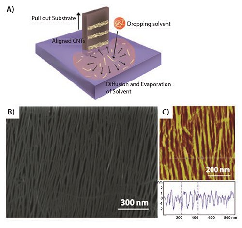
In collaboration with Padma Gopalan’s group at the University of Wisconsin-Madison, we recently demonstrated progress in increasing the on/off ratio and on-conductance of PFO-BPy sorted s-SWCNT FETs by aligning the SWCNTs with a technique we pioneered called Floating Evaporative Self-Assembly (FESA).29 In FESA, a substrate is withdrawn from an aqueous sub-phase, onto which small droplets of SWCNT “ink” (namely, polymer-wrapped SWCNTs dissolved in chloroform) are delivered in the vicinity of the substrate (schematically depicted in Figure 3A). The ink spreads rapidly across the water surface and a thin film wets the substrate. This volatile ink film evaporates quickly and deposits a stripe of aligned, unbundled s-SWCNTs that spans the width of the substrate. The spacing of the stripes and the density of the SWCNTs within each stripe can be controlled through the deposition parameters. Scanning electron microscopy (SEM) and atomic force microscopy (AFM) images of aligned SWCNTs within a single stripe are presented in Figures 3B–C, where the AFM height profile indicates the film consists of an approximate monolayer of individualized SWCNTs. Overall, the result of FESA is the rapid deposition of SWCNTs into aligned arrays that can be adapted for scalable integration into a wide variety of microelectronic applications.

Figure 3.Alignment and film characteristics of SWCNTs prepared via Floating Evaporative Selfassembly. A) Schematic of the FESA experimental process. B) SEM image of aligned SWCNTs fabricated by FESA deposition. C) Atomic Force Microscopy tapping mode image of aligned SWCNTs. Inset height profile along the cross-section of the aligned SWCNTs indicates a monolayer of isolated SWCNTs. Adapted with permission from Reference 29, copyright 2014, American Chemical Society.
High-Performance Transistors
We leveraged our work on FESA to fabricate the highest performance nanotube FETs to date, using the on-conductance and on/off ratio as key metrics.16 The source-drain current of an aligned SWCNT FET is plotted as a function of gate-voltage in Figure 2B. The measurement is used to extract values for on-conductance and on/off ratio of 260 μS/μm and 2×10⁵, respectively.16 As shown in Figure 2C, compared to previous stateof-the-art SWCNT FETs, we achieved significant performance gains in on/off ratio and on-conductance.16,19,20,22,23,25,28,30–35 We observed a 1,400-fold increase in on/off ratio compared to previous state-of-the-art SWCNT FETs with on-conductance per width of 250 μS/μm. Likewise, 30–100 fold greater on-conductance per width was achieved when compared to state-of-the-art high on/off ratio SWCNT FETs. The excellent performance of the devices resulted from the high semiconducting purity and the high degree of alignment of the SWCNT arrays. Moreover, the excellent performance was due to the SWCNTs remaining isolated and unbundled during their deposition, which minimized detrimental crosstalk between SWCNTs and improved the electrode/SWCNT contacts. Additionally, we used these FET arrays to measure the semiconducting purity based on the magnitude of the on/off ratio. These FETs contain 5,519 SWCNTs all having an on/off ratio greater than 5×10³, indicating that the semiconducting purity is at least 99.98%. These results highlight the promise of aligned polyfluorene-sorted SWCNTs and FESA for nextgeneration thin film FET and computing applications.
Flexible and Stretchable Transistors
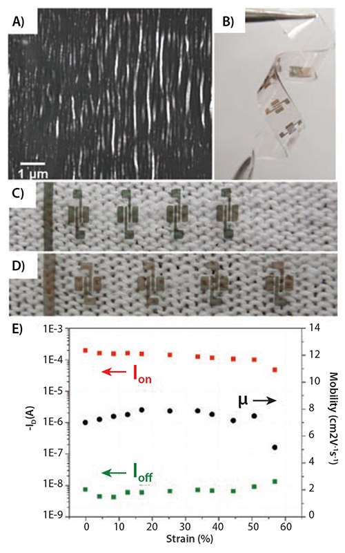
The excellent mechanical resilience36 of SWCNTs opens the door for their use in new types of electronic devices and circuits that are not confined to rigid substrates but can be integrated on flexible, elastomeric, or unconventional substrates like clothing, paper, or biological tissue that can flex, bend, and even stretch.37–39 To fabricate highly flexible and stretchable thin film FETs, it is important to consider the mechanical behaviors of all of the components including the channel, electrodes, and dielectric, and the interfaces between them, under deformation. Our group fabricated highly stretchable FETs by depositing random networks of PFO sorted s-SWCNTs onto pre-stretched elastomer substrates and buckling the network thin films by releasing the strain.40 The contacts are composed of buckled gold/chromium thin films, and a polymeric ionic conductor is used as a flexible dielectric. The FETs fabricated in this way can operate under strain of over 50% without sacrificing electrical performance in on/off ratio or mobility,40 as shown in Figure 4.

Figure 4.A) SEM image of buckled s-oSWCNT film after release of pre-strain and demonstration of B) flexibility and C,D) stretchability. E) On (Ion) and off (Ioff) currents and mobility (μ) versus strain of the stretchable FETs. Adapted with permission from Reference 40, copyright 2014 American Chemical Society.
Carbon Nanotube Optoelectronics
Device Operation
s-SWCNTs are promising photoabsorbers for next-generation photovoltaic solar cells and photodetectors because they are strong optical absorbers with tunable bandgaps, transport energy and charge on ultrafast timescales, are relatively chemically stable, and are solution-processable. The application of s-SWCNTs as the efficient light-absorbing component of photovoltaic devices has only recently been possible with the advent of methods for eliminating m-SWCNTs, which otherwise are known to quench photoexcitations in nearby s-SWCNTs.
One challenge is that optical absorption in s-SWCNTs produces electronhole pairs known as excitons. The electrons and holes in the excitons are bound to each other with an energy that is >100 meV, significantly above thermal energy at room temperature, suppressing their spontaneous dissociation and separation into free charges that are needed to produce electrical energy.41 We have shown that it is possible to overcome the exciton binding energy by pairing thin films of s-SWCNTs with other semiconductors to create heterojunctions.42 The heterojunction must have a band offset exceeding the exciton binding energy to allow efficient exciton dissociation. For example, fullerene-C60 (Prod. Nos. 572500, 379646 and 483036) is an excellent electron acceptor for thin films of large bandgap polyfluorene-sorted s-SWCNTs, including (6,5), (7,5), (7,6), and (8,6) chiralities. The internal quantum efficiency (IQE), which quantifies the fraction of absorbed photons that result in separated electron-hole pairs that are collected at the device contacts at zero-bias, is >85% for these species when the SWCNT film thickness is less than ~5 nm.43 The IQE of the SWCNT/C60 heterojunction decreases to less than 50% when the (8,7) and (9,7) SWCNTs are used due to a decreasing band offset and a lower driving force for exciton dissociation.44
Another factor that influences IQE is the exciton diffusion length. In a bilayer heterojunction device, photogenerated excitons must diffuse to the SWCNT/C60 heterointerface (where dissociation will take place) before the excitons recombine and are lost as heat. Excitons can diffuse either along the long-axis of SWCNTs (intra-tube) or transfer between SWCNTs (inter-tube). In solution-cast SWCNT films, the SWCNTs adopt a lying-down morphology. Exciton diffusion to the C60 layer must occur via inter-tube hopping. During inter-tube hopping, excitons tend to hop from large to small bandgap species (i.e., downhill energy transfer). Because small bandgap nanotubes are less efficient donors and trap excitons, it is important to avoid them, in addition to avoiding m-SWCNTs. In a recent modeling study, we found that the chirality distribution of s-SWCNTs can significantly influence the exciton diffusion length,45 with the longest exciton diffusion lengths predicted for films of nearly monochiral s-SWCNTs.
Recent Advances
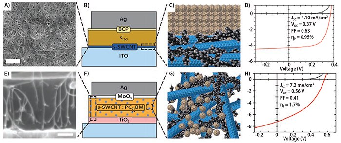
Using nearly monochiral films of (7,5) SWCNTs, Bindl et al. reported a monochromatic power conversion efficiency of 7.1% at the S1 transition of the (7,5) nanotube.46 Later optimization by Shea et al. yielded a power conversion efficiency of nearly 1.0% (Figures 5A–D) under simulated solar irradiation (AM1.5G).47 Of particular note is that the photoabsorbing SWCNT films driving the power conversion in these devices are only several nanometers thick. One may expect that an increase in SWCNT film thickness would yield a corresponding increase in power conversion efficiency. However, Bindl and Shea et al. noted that the optimized external quantum efficiency and power conversion lies at s-SWCNT film thickness of 5–8 nm. It is believed that the short inter-tube exciton diffusion length48 (discussed previously) limits the maximum film thickness achievable before decreased exciton diffusion efficiency outweighs any increase in absorption obtained from a thicker film.
A common method to avoid the problem of short exciton diffusion length is to fabricate bulk or blended heterojunction devices where the acceptor material is never more than an exciton diffusion length away from a photogenerated exciton in the donor. Most polymer bulk heterojunction (BHJ) devices are fabricated by casting solutions containing both a polymer donor such as P3HT and a fullerene-derivative acceptor at similar concentration. One complication associated with replacing the common P3HT:fullerene BHJ with a SWCNT:fullerene analog is the relatively low solubility of PFO-wrapped SWCNTs compared to small molecule fullerene-derivative electron acceptors. Ye et al. developed one solution to this problem by fabricating s-SWCNT aerogels and filling the aerogels with a fullerene-derivative solution.49 In this way, significantly higher optical density at the SWCNT transitions were achieved without limiting exciton diffusion pathways. Ye et al. reported a maximum AM1.5G power conversion efficiency of 1.7% (Figures 5E–H). Others have also recently reported exciting progress towards the use of s-SWCNTs in the light-absorbing components of solar cells50,51 and photodetectors.52

Figure 5.A) Scanning electron micrograph of a film of s-SWCNTs. The scale bar is 200 nm. B,C) Device schematic for bilayer s-SWCNT/C60 heterojunction solar cell. D) Bilayer solar cell performance under AM1.5G illumination. Adapted with permission from Reference 47, copyright 2013 American Institute of Physics. E) Cross-section micrograph of bulk heterojunction fabricated by intercalation of s-SWCNT aerogel by PC71BM. The scale bar is 100 nm. F,G) Device schematic for bulk heterojunction s-SWCNT:PC71BM solar cell. H) Solar cell performance under AM1.5G illumination. Adapted with permission from Reference 49, copyright 2014 Wiley.
Conclusion
Polyfluorene sorting provides a simple, scalable method to achieve s-SWCNTs for electronic and optoelectronic applications. With electronictype purity of at least 99.98%, s-SWCNTs isolated by this process are appealing materials for a number of next-generation electronic and optoelectronic devices. Our group has specialized in incorporating polyfluorene-sorted s-SWCNTs in high performance FETs, flexible and stretchable devices, and as the photoabsorbing material in solar cells and photodetectors. Advances in isolation and processing will continue to improve the performance of SWCNT-based devices and advance knowledge of the properties and behaviors of these one-dimensional materials.
Acknowledgments
Support is acknowledged from the National Science Foundation (CMMI-1129802), the University of Wisconsin National Science Foundation Materials Research Science and Engineering Center (MRSEC) (DMR-1121288), the National Science Foundation (DMR-1350537), the U.S. Army Research Office (W911NF-12-1-0025), and the Air Force Office of Scientific Research (FA9550-12-1-0063). GJB also acknowledges support from the National Science Foundation Graduate Research Fellowship Program under Grant No. DGE-1256259.
Materials
References
如要继续阅读,请登录或创建帐户。
暂无帐户?