Electronic and Biomedical Applications of High-Purity Single-Walled Nanotubes (SWNTs)
SWNT Structure & Growth
Carbon Nanotubes (CNTs) are stable, hollow cylinders of pure carbon closely related to graphite, graphene and fullerenes.1 CNTs can be visualized by taking a single graphene sheet and rolling it into a tube with a diameter on the nanometer scale. CNTs are commonly classified into two categories, single walled carbon nanotubes (SWNTs) and multi-walled carbon nanotubes (MWNTs). MWNTs contain multiple concentric nanotubes with inherently a higher degree of impurities and defects. MWNTs are poorly suited for electronic applications due to their high optical absorbance and insufficient band gap (arising from their larger diameter). SWNTs generally have fewer defects and a higher degree of crystallinity than MWNTs, giving rise to superior performance in most applications. The diameter and degree of twist of SWNTs have a dramatic effect on their electronic properties, causing some nanotubes to behave as metallic conductors and others as direct band gap semiconductors. The nanometer scale structure of SWNTs leads to extraordinary mechanical2, thermal2, electrical3 and optical3 properties. This unique combination of properties has made SWNTs the subject of promising research and development in areas as diverse as composites, coatings, packaging, solar cells and displays.
SWNTs occur naturally on Earth in very small amounts, but can be synthetically produced in much larger quantities using three basic components: a catalyst, carbon and energy. Their synthesis can be tailored by control over the carbon source, catalyst type and growth conditions. There are several major techniques4 for growing carbon nanotubes, each of which possess different advantages. For many electronic applications, SWNTs with a mean diameter of ~1.5 nm have been shown to give optimal performance. However, many growth techniques yield mixtures of SWNTs and MWNTs, wide diameter distributions or small mean diameter tubes (< 1nm). Arc discharge, laser vaporization and induction thermal plasma processes have been shown to give high quality SWNTs in the desired ~1.5 nm diameter range, without the presence of MWNTs. These processes have some similarities such as high temperature, low pressure and catalyst type. However, the plasma torch process has proven to be the most scalable, with demonstrated production capacity of > 1kg/day of SWNTs and potential for further scale-up.5
Purification & Separation
One significant challenge with all current CNT growth processes is the inherent formation of impurities as well as a diverse mixture of different types of nanotubes. Carbon nanotubes grown via the plasma torch process contain a significant amount of impurity particles that are shown in Figure I (a).6 Furthermore, as-prepared SWNTs contain a polydisperse mixture in length, diameter, electronic type, chirality and chiral handedness. Figure 1 (b) illustrates the CNT polydispersity problem.7
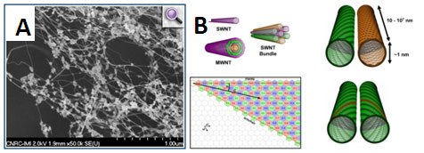
Figure 1. (a) As-Grown CNTs from RF Plasma Growth Process6 (b) Schematic showing the polydispersity of CNTs7 (Figure was adapted from references 6 and 7)
The presence of impurities and CNT polydispersity pose challenges to achieving high-performing nanotube devices. Mixtures of metallic and semiconducting SWNTs can dramatically degrade device performance in electronic applications because metallic tubes will short semiconducting devices. Both high purity and homogeneous electronic type are required in order to achieve the performance potential of SWNTs. Therefore, as produced SWNTs must be purified to remove impurities and then separated to isolate monodisperse samples. A breakthrough method for achieving SWNT separation was pioneered by Arnold and Hersam in 20068, which offered significant advantages over alternative techniques7. This separation process is known as Density Gradient Ultracentrifugation (DGU), and has successfully been applied to sort CNTs by the number of walls, diameter, electronic type, chirality and chiral handedness (left- vs. right-handed SWNTs). First, CNTs are solubilized in water using specialized surfactants that bind preferentially to specific types of CNTs. Next, CNTs are separated by centrifuging the solution in a density gradient until the nanotubes reach their equal-density positions within the gradient and can be physically isolated.
The DGU process was commercialized and scaled up by NanoIntegris to produce purified and separated carbon nanotubes. The properties of these materials are shown in Table 1.
Purified and unsorted SWNTs offer superior purity compared to as produced CNTs. Solutions of these PureTubes™ nanotubes have a brown-gray color, compared with the black buckypaper as shown in Figure 2(a). The enhanced purity of this material can be clearly visualized by the optical absorbance spectra for PureTubesTM vs. traditionally purified CNTs prepared by arc discharge as shown in Figure 2(b). The degree of purity can be determined by calculating the peak-to-background ratios of each material and comparing these ratios to a highly purified sample. The peaks arise from the electronic transitions of the SWNTs, while the sloping background comes primarily from impurities (scattering and p-plasmon absorption). These electronic transitions arise from the one-dimensional density of states (van Hove singularities) of the SWNTs and occur at different energies for metallic (M11) and semiconducting (S11, S22, and S33) nanotubes.
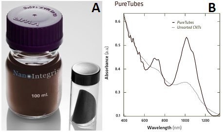
Figure 2. (a) PureTubes solution and buckypaper and (b) Optical Absorbance characterization showing dramatically improved peak:background ratio compared with standard unsorted SWNTs.
There are many other techniques for characterizing SWNTs (including Raman, OA, PL, TGA, EA, SEM/TEM, etc.) and a full list of characterization data can be found in the technical data sheet9. There are two grades of Purified SWNTs: PureTubesTM (<3.5% catalyst content, Prod. No.750492) and SuperPureTubesTM (<1% catalyst content, Prod. No.750514). These purified SWNTs offer improved performance in most applications compared with as-produced CNTs.
For most electronic applications, SWNTs must be pure and highly enriched with respect to electronic type (metallic or semiconducting). Following purification, SWNTs can be separated by electronic type to produce metallic
(IsoNanotubes-MTM, Prod. No.750530) and semiconducting SWNTs (IsoNanotubes-STM, Prod. No.750522). The degree of electronic type enrichment can be measured using optical absorbance by comparing the relative heights of the metallic M11 peaks (550-800nm) with the semiconducting S22 (850-1250nm) and S33 (450-550nm) peaks.
A typical optical absorbance spectrum for IsoNanotubes-M (98% metallic) shows a pronounced peak in the M11 region and an absence of peaks in the S22 and S33 regions (Figure 3). The spectrum also displays a high peak-to-background ratio, consistent with exceptionally high SWNT purity.
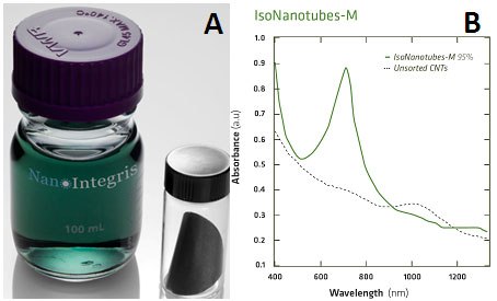
Figure 3. (a) IsoNanotubes-MTM solution and buckypaper and (b) Optical Absorbance spectrum showing characteristic metallic M11 peak and high peak-to-background ratio compared with standard unsorted SWNTs.
Metallic nanotubes are useful for applications where electrical conductivity is important, such as conductive composites or transparent conductive films10 for touch screens, displays and photovoltaics.
A typical optical absorbance spectrum for IsoNanotubes-S (~98% semiconducting) is shown in Figure 4, with clear peaks in the S22 & S33 regions and an absence of peaks in the M11 range. Similar to the PureTubesTM and IsoNanotubes-MTM, this spectrum also shows a high peak-to-background ratio. Semiconducting SWNT such as IsoNanotubes-STM are utilized in electronic and optoelectronic devices where semiconductor materials are required.
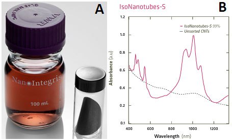
Figure 4. (a) IsoNanotubes-S TM solution and buckypaper and (b) Optical Absorbance spectrum showing characteristic semiconducting S22 and S33 peaks and high peak-to-background ratio
Electronic Applications
There are a wide variety of potential applications for high purity SWNTs where researchers are exploring their unique structure and properties.11 For electronic applications, semiconducting SWNTs (s-SWNTs) have received significant attention as the active layer in thin film transistors (TFT).12 Commercial availability of s-SWNTs [IsoNanotubes-STM (Prod. No. 750522)] has helped accelerate progress in this area, leading to increased performance (mobility, on/off ratio, etc.). Figure 5 illustrates the use of CNT-TFTs for OLED backplane transistors, with performance comparable to TFTs made from polycrystalline silicon or Indium Gallium Zinc Oxide (IGZO).13
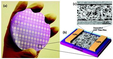
Figure 5. (a) The wafer consists of CNT-TFTs (b) Schematic showing CNT-TFT (c) SEM image showing CNT network of IsoNanotubes-S TM (Figure was adapted from reference 13)
In this application, enriched s-SWNTs give enhanced mobility (~10-100 cm2/V-s) and an on/off ratio of 103 – 106, which are critical for peak device performance. Due to their combination of mechanical and electronic properties, semiconducting CNTs are promising materials for printable and flexible electronics. Recently, TFTs containing IsoNanotubes-STM (Prod. No. 750522) were used as the backplane for a bendable pressure sensor (Figure 6).14 This ‘artificial skin’ device is just one example of the new types of wearable and flexible devices that are being developed.
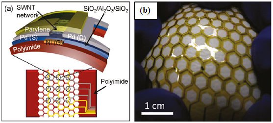
Figure 6. (a) Schematic and (b) Photograph of stretchable pressure sensor using IsoNanotubes-S TM for the backplane TFT. 14 (Figure was adapted from reference 14)
Nanotube TFTs are also being explored for use in a variety of different semiconductor devices, including analog radio frequency (RF) devices,15,16 printed radio-frequency identification (RFID) chips,17 radiation-hardened electronics,18 CMOS logic19 and chemical & biological sensing.20 Semiconducting nanotubes have also been used in the active layer of photo-detectors and photovoltaic cells.21
Biomedical Applications
There is growing interest in utilizing carbon nanotubes for a variety of biomedical applications that take advantage of the structural and optical properties of CNTs. One approach is to use the nanotubes as vehicles for more efficient and targeted drug delivery, potentially allowing for improved cancer therapies due to lower drug dosage and reduced systemic side effects.22 Alternatively, researchers have prepared functionalized CNTs so that they can be readily absorbed by cancer cells, and then selectively heated the CNTs using NIR light (700-1100nm). The CNTs preferentially absorb the radiation and transfer the heat to their surroundings, causing localized cell death.23 CNTs have also been utilized for biomedical imaging by monitoring the photoluminescence of the CNTs as they circulate in a mouse, illustrated in Figure 7.24
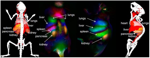
Figure 7. Dynamic Contrast Image of a mouse using functionalized SWNTs and Principal Component Analysis24 (Figure was adapted from reference 24)
Summary
Innovative research approaches using highly purified SWNTs continue to grow: semiconducting carbon nanotubes may one day replace or complement traditional semiconductors in both high-performance and low-cost thin film transistor (TFT) devices. Uniform metallic CNTs, as an alternative to ITO, may become an integral component of many devices, including electrochromic glass, solar panels and LCD and OLED displays. Well defined semiconducting SWNTs represent a "smart" nanotechnology platform and may prove useful for targeted drug delivery with higher efficiency and reduced systemic side-effects.
Materials
References
To continue reading please sign in or create an account.
Don't Have An Account?