Self-Assembled Nanodielectrics (SANDs) for Unconventional Electronics
Introduction
The field of unconventional electronics represents a new opportunity for the semiconductor and electronics industries.1 This broad field encompasses both “printed organic/inorganic” and “transparent” electronics. The first technology aims at the fabrication of extremely cheap electronic devices such rf-id tags, ‘smart’ cards, flexible electronic paper, and backplane circuitry for active matrix displays by high throughput manufacturing, while the second targets “invisible” devices such as transparent circuits and monitors. The key component of all modern electronics is the thin-film transistor (TFT, See Figure 1 for structure and function). The three fundamental TFT materials components are the contacts (source, drain, and gate), the semiconductor, and the gate dielectric.

Figure 1.Structure and operation of a thin-film transistor. The basic equation describing the TFT drain current in saturation is ISD = (W/2L) μCi (VSG-VT)2 (eq. 1), where μ is the field-effect carrier mobility of the semiconductor, W the channel width, L the channel length, Ci the capacitance per unit area of the dielectric layer, VT the threshold voltage, VSD the drain voltage, and VG the gate voltage. In contrast to conventional Si transistors, organic TFTs normally operate in the accumulation mode, where applying a gate voltage creates mobile charge carriers in the channel, thus switching the device “on”. The semiconductor field-effect mobility is calculated from the I-V data according to eq. 1. The device current Ion:Ioff ratio, and the subthreshold slope (related to how efficiently the gate field modulates the off to on current and how crisply the device turns on) are also important TFT performance characteristics.
While much of the attention has been focused on the search for highmobility, stable, and possibly printable/transparent semiconductors, it is now clear that the use of a proper gate dielectric is necessary to optimize device performance. Self-assembled nanodielectrics (SANDs) are gaining significant attention as gate dielectrics due to their robust insulating properties, tunable thicknesses at the nanometer level, optical transparency in the visible range, and efficient solution processability. In this article, we survey basic SAND structure, function, and implementation with a variety of semiconductors for TFT fabrication.2
SAND Chemistry, Fabrication, and Properties
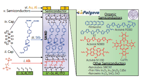
Traditionally, organic/transparent TFTs have been fabricated using a 100-300 nm thick SiO2 (Product No. 637246) insulating layer as the gate dielectric.3 This material prevents current leakage between the source/drain contacts and the gate, and allows accurate electrical performance characterization of the semiconducting layer. A major motivation to search for alternative gate dielectrics is to enable inexpensive TFT fabrication and to significantly reduce the operating voltages. Lower operating voltages mean lower power consumption and batteries more compatible with portable electronics. According to equation 1 (Figure 1 caption), a viable approach to substantially increase TFT source-drain current (ISD) while operating at low biases is to increase the capacitance of the gate dielectric, Ci = ε0(k/d), where k is the dielectric constant of the material, and d the insulator thickness. Importantly, alternative TFT gate dielectrics such as SAND must not only have large capacitance but also exhibit acceptable (<1% of the ISD) gate leakage currents. SAND dielectrics are a type of self-assembled multilayers, which are composed of ordered molecular assemblies formed by the spontaneous adsorption of active molecular precursor(s) onto solid surfaces. Usually the precursor molecular species are sequentially deposited from common organic solvents. In the case of SAND fabrication, organosilane molecules (Alk, Stb, and Cap, Figure 2) are employed. This self-assembly chemistry requires hydroxylated substrate surfaces, such as those of the technologically relevant SiO2, Al2O3, (Product No. 642991) and indium tin doped oxide (ITO) (Product No. 544876) surfaces. The driving force for self-assembly is in the in situ formation of siloxane linkages, which connects the precursor silane to the surface hydroxyl (-OH) groups via strong covalent -Si-O- bonds. The present method for SAND fabrication involves iterative application of (Figure 2): (a) Self-assembled α,ω- difunctionalized hydrocarbon chains [Cl3Si(CH2)nSiCl3] (Alk). Difunctional hydrocarbon monolayers undergo transverse crosslinking, enabling precision, stepwise layer build-up, increasing interchain packing and reducing defects/pinholes. (b) Highly polarizable “push-pull” stilbazolium layers (Stb). Self-assembled, oriented π-electron dipolar layers stabilize charge carriers in the proximate semiconducting channel when the device is turned on (VG ≠ 0). (c) Octachlorotrisiloxane capping layers (Cap). Multilayer structural robustness can be further enhanced by capping/planarizing with a highly crosslinked, glassy siloxane polymer.

Figure 2.Left: Schematic representation of the components of a thin-film transistor (TFT) with the indicated the self-assembled nanodielectric (SAND) structure of Type III (right) on highly doped Si(100), Al, or ITO substrates/gate electrodes. Nanodielectric layers (5.5 nm thick for Type III SAND) are then sequentially deposited from solutions via layer-by-layer deposition of silane precursors Alk, Stb, or Cap (left), following the procedure from step i. to iv. The OTFT device is completed by deposition of the semiconductor (step v) and finally by the source-drain electrodes (step vi). Right: Chemical structure of some p- (blue) and n-type (red) organic semiconductors used with SANDs (some of them are commercially available at www.polyera.com) as well as a selection of other semiconductors employed to fabricate SAND-based TFTs.
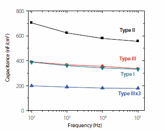
Different types of SAND multilayer structures can be obtained (and were studied) by various layer percursor combinations. The most common SANDs are identified by the following nomenclature: Alk+Cap layers (Type I), Stb+Cap layers (Type II), and Alk+Cap+Stb+Cap layers(Type III). The most used SAND for the fabrication of TFTs with organic semiconductors is Type III (~5.5 nm thick) whereas for inorganic semiconductor-based TFTs, the one used most is a trilayer of Type III (Type IIIx3, ~16 nm thick). The microstructures and electrical properties of SANDs have been characterized by x-ray reflectivity, optical absorption spectroscopy, optical second-harmonic generation measurements, atomic force microscopy, and scanning electron microscopy. SANDs were established as excellent, pinhole-free insulators via solution-phase cyclic voltammetry and MIS leakage current measurements (current densities ~10-8-10-5 A/cm2), and measured breakdown fields were ~5-7 MVcm-1. Capacitance-voltage (C-V) measurements on MIS structures reveal maximum capacitances Ci = 400 (I); 710 (II); 390 (III), ~180 (Type IIIx3) nFcm-2 at 102 Hz (Figure 3) vs. ~11 nFcm-2 for 300 nm-thick SiO2.

Figure 3.Frequency (f) dependence of the capacitance in the accumulation regime (1.0 V) between 102 - 105 Hz for the indicated SAND nanodielectrics.
Thus, considerable TFT driving voltage reduction is possible (vide infra). Recently, it was found that the annealing of I-III at 120-180 °C reduces C-V hysteresis and frequency-dependent C-V dispersion. SAND Type IIIx3 films are also exceptionally thermally stable, and the annealing of these films at 400 °C enhances dielectric strength, reduces current leakage, and increases capacitance, thus opening unprecedented opportunities for integration with high-temperature processed inorganic semiconductors.
Organic Semiconductor-SAND Transistors
First-generation SAND-based organic TFTs were fabricated on doped silicon substrates (gates) using a variety of organic semiconductors discovered/developed at Northwestern University and Polyera Corporation.5,6 In initial studies, the semiconductor layer was deposited by vapor deposition or spin-coating, and the device structure was completed by Au source/drain deposition. However, recent work at Polyera demonstrates that inkjet printing of the semiconductor on SANDs is possible. The investigated semiconductors include various pentacenes, oligothiophenes, polythiophenes, metallophthalocyanines, and perylenes. All SAND-organic semiconductor-based devices exhibit reproducible I-V characteristics at very low biases with classical linear and saturation response properties, as exemplified by data for typical p-type (hole conductor; Polyera ActivInk P0300) and n-type (electron conductor; Polyera ActivInk N1200) organic semiconductors (Figure 4).

Figure 4.Performance output characteristics as a function of gate voltage (VG) for SAND-based organic transistors with p-channel (ActivInk P0300) and n-channel (ActivInk N1200) organic semiconductors.
In marked contrast to these results, control devices fabricated with the commonly used SiO2 dielectric (300 nm thick, Ci ~11 nF/cm2) exhibit no useful source-drain current modulation over these same voltage ranges. Carrier mobilities for these semiconductors are similar to those obtained on Si-SiO2 substrates, ~0.1 cm2/Vs for both ActivInk P0300 and ActivInk N1200. Note that also TFTs fabricated on ITO-coated glass gates function comparably, demonstrating that a Si/SiO2 native oxide gate electrode is not required to achieve excellent dielectric performance. Finally, these nanodielectrics can be used to fabricate flexible TFTs on commercially-available ITO-coated plastic (Mylar) gates, demonstrating applicability to flexible plastic electronics.
Inorganic Semiconductor-SAND Transistors and Circuits
We next investigated SAND compatibility with semiconductors other than small organic molecules. We first demonstrated the compatibility of Type IIIx3 SAND with single-wall carbon nanotubes (SWCNTs) (Product No. 704113, 704121, 704148) as the semiconductor.7 SWCNTs where grown by CVD onto SiO2/Si wafers and transfer printed (~10 tubes/μm2) directly onto the Si-SAND substrates (and control Si/SiO2 substrates). Good SWNT-SAND adhesion allows direct photolithographic patterning of the source and drain electrodes by liftoff. It is found that TFT performance is significantly improved over control devices using 100 nm Si/SiO2 gate dielectrics, with substantially lowered hysteresis and VT shifts. Thus, the TFT mobility is excellent with μhole ~5.6 cm2/Vs, VT = 0.2 V, and a low gate leakage current of ~10 nA at VG = -1 V demonstrated. Furthermore, compatibility with n-type SWCNTs (those having a PEI coating) is demonstrated, with small observed hysteresis and TFT properties: μelectron = 4.1 cm2/Vs and VT = -2 V. Compatibility of SAND dielectrics with thin-film inorganic semiconductors was demonstrated by using In2O3 thin-films (Product No. 203424) to enable high-performance, low-voltage, and fully transparent TFTs.8 In2O3 is a wide-bandgap (3.6-3.75 eV) n-type semiconductor with excellent transparency in the visible region (>90%). Thin films of In2O3 were deposited at room temperature by ion-assisted deposition (IAD) directly on top of the SAND dielectric, and device fabrication completed by Au source/drain contact deposition. Note that the SAND is stable to the in-situ ion/plasma exposure during In2O3 deposition. Significant In2O3 TFT performance enhancement is observed with SAND-gated devices, where μ = 140 cm2/Vs, interfacial trap density, D = 1011 cm-2, VT = 0.0 V (with nearly hysteretic free response), on/off = 105, and the subthreshold slope = 150 mV/decade. These metrics can be compared to the performance on Si/SiO2-gated devices where μ = 10 cm2/Vs and on/off = 105. To realize fully transparent TFTs, the same fabrication procedures were followed except utilizing glass/ITO as the bottom gate electrode and doped In2O3 source and drain electrodes. The performance of SAND-based transparent TFTs is essentially the same as on n+-Si substrates but with an improved subthreshold slope = 90 mV/decade.
The versatility of SAND as an effective gate dielectric for non-organic semiconductors was further demonstrated in TFTs using ZnO, In2O3, and SnO nanowires (NWs).9 As an example, ZnO NW (nanowire) TFTs with SAND IIIx3 as the gate dielectric were fabricated with ZnO nanowires (80 nm average diameter, and 5 μM average length) dispersed in 2-propanol (Product No. 278475) and then transferred to the SAND-coated Si substrates. Source and drain Al electrodes were deposited by electron beam evaporation and patterned by photolithography. The SAND dielectrics were first electrically characterized in MIS devices (Al/SAND/Si), where a leakage current density of ~10-8 A/cm2 was measured, verifying SAND compatibility with the photolithographic and e-beam evaporation methodologies. SAND gated ZnO2 NW-TFTs reduced operating voltages to <1.5 V (from >1.5 V on Si/SiO2), while maintaining the device on/off ratio, increasing the on-current to 2 μA (from 0.3 μA), and increasing the mobility and transconductance. The VT of SAND gated ZnO NW-TFTs is -0.4 V, and the subthreshold slope is 400 mV/decade. High subthreshold slopes usually indicate surface traps, so the SAND-based ZnO NW-TFTs were then treated with ozone exposures, and indeed the subthreshold slope was reduced to 150 mV/decade. In addition, reduced VT values (0.2 V) and improved on:off ratios (108) were observed. The calculated electron mobility (taking into account the cylindrical geometry of the channel) is 196 cm2/Vs, which is far greater than 8-18 cm2/Vs measured for ZnO NW on thick Si/SiO2 dielectrics, and 54 cm2/Vs for a 70 nm thick SiO2 control dielectric. The TFT mobility varies from 164-181 cm2/Vs with variations in NW diameter and length. One of the remarkable properties of SANDbased electronics is their resistance to radiation damage, known as radiation hardness. The proton (10 MeV H+) radiation tolerance was investigated first for SAND IIIx3/ZnO-NW TFTs.10 After various dosing and exposure conditions in a nuclear reactor, neither the leakage current nor the VT of the SAND-gated TFTs shifts significantly. Currently SAND-gated organic and inorganic TFTs are on the International Space Station for additional radiation testing. These results suggested that the bulk oxide trap density and interface trap density formed in SAND (or at the SAND-ZnO NW interface) during H+ irradiation are significantly lower than in traditional SiO2 gate dielectrics. This prompted detailed studies of ZnO-NW TFTs using low-frequency noise and temperaturedependent I-V measurements to characterize the surface/interface states. Lower 1/f noise constants are found for SAND-based devices compared to SiO2-based devices, and it is concluded that the interface trap densities are comparable to those for the aforementioned SWCNT devices (D = ~1012 cm2V-1) by comparison of the Hooge’s constant metric. Larger temperature variations of the transfer curves, and larger threshold voltage shifts vs. temperature observed for SiO2/ZnO-NW TFTs versus the corresponding SAND-gated devices, provide further evidence that the SAND/ZnO-NW TFTs have exceptionally low interface trap and defect densities.
All of the processes described above demonstrate that SANDs are robust gate dielectrics compatible with a number of inorganic semiconductors. However, since the above semiconductor depositions were all carried out near room temperature, the question arises as to whether SAND is stable at higher temperatures. Very recently we demonstrated that SAND IIIx3 films are stable to 400 °C, thus opening a broad range of processing possibilities at high temperatures.11 One particular challenge has been to implement organic dielectric materials with aqueous solution-processed inorganic semiconductors. To achieve this, we explored the compatibility of SAND-based TFTs with solutionprocessed cadmium selenide (CdSe) (Product No. 244600), In2O3, and ITO as the semiconducting layers. As an example, the chemical bath deposition method was recently used to deposit the CdSe films on SAND IIIx3 gate dielectric layers. Optimum performance of on:off ratio = 106, VT = 3.0 V, and subthreshold slope = 0.26 V/decade was achieved for CdSe/SAND-based TFTs annealed at 400 oC, which exhibit mobilities of ~40 cm2/Vs vs. ~4 cm2/Vs for the analogous SiO2-based devices. Excellent performance was also achieved with In2O3 12 and ITO as the TFT semiconductors.
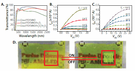
Finally, we demonstrated the application of SAND/nanowire technology to realize fully transparent circuitry based on ZnO and In2O3 nanowires and ITO or AZO (Al-Zn-O) source/drain/gate contacts.13 From this starting point, active matrix organic light-emitting diode (AMOLED) displays were fabricated with switching and driving circuits comprised exclusively of nanowire transistor (NWT) electronics fabricated at room temperature (Figure 5). The mobilities of these SAND-based In2O3 NW TFTs are ~160 cm2/Vs, sufficient to drive bright display pixels. Fully transparent, proof-of-concept 2 x 2 mm NW-AMOLED arrays (300 pixels = 900 NWTs) were fabricated using very thin Al cathodes on glass substrates.12 The optical transmission values are ~72% (before OLED deposition) and ~35% (after OLED deposition; thinner Al is required) in the 350-1350 nm wavelength range, which corresponds to a green peak luminescence of >300 cd/m2. Note that transmission coefficients up to 70% have been reported for OLED structures on plastic substrates, although values in the 50% range are more common.

Figure 5.Optical transmittance of multilayer films used to fabricate transparent TFTs based on SAND gate dielectrics and a thin film of In2O3. B, C. Output transistor characteristics of IAD In2O3 thin film with SAND (B) and SiO2 (C). Note the difference in the operating voltages. D. Partially transparent active-matrix organic LED display based on nanowire electronics.
Conclusions
In this short account, we briefly summarized the potential and promise of self-assembled multilayer gate dielectric films fabricated from silane precursors for organic, inorganic, and transparent TFTs, as well as for TFT circuitry and OLED displays. These materials illustrate the potential of molecular chemistry for constructing unusual and useful electronic materials.
Acknowledgments
We thank ONR (N00014-05-1-0766), AFOSR (FA9550-08-1-0331), and Polyera Corp. for support of this research, and the NSF-MRSEC program through the Northwestern University Materials Research Science and Engineering Center (DMR-0520513) for providing both support and characterization facilities. We thank all of our collaborators for the important and enthusiastic contributions to this work.
Materials
References
To continue reading please sign in or create an account.
Don't Have An Account?