
793353
Tungsten oxide (WO3-x) nanoparticle ink
Synonym(s):
Tungsten oxide nanoparticle dispersion, Tungsten oxide suspension, WO3 dispersion, WO3 ink, Tungsten oxide, Tungsten oxide nanoparticle
Sign In to View Organizational & Contract Pricing.
Select a Size
Change View
About This Item
Linear Formula:
WO3-x
NACRES:
NA.23
UNSPSC Code:
12352103
form
dispersion
Quality Segment
concentration
2.5 wt. % in 2-propanol
particle size
<50 nm (BET)
density
0.7992 g/mL at 25 °C
General description
This WO3-x nanoparticle ink is for slot-dye, spin-coating and doctor blading for the use as hole transport layer in printed electronics. Tungsten oxide nanoparticle ink is a hole-selective interface layer ink based on a colloidal suspension of tungsten oxide (WO3) nanoparticles in isopropanol. The average size of WO3 particle is optimized around 12-16 nm. Tungsten oxide nanoparticle exhibits high work function, processability and easy layer formation on hydrophilic as well as hydrophobic substrates.This WO3-x nanoparticle ink is universally applicable in normal and inverted architecture solar cells.
Annealing temperature <100°C.
Annealing temperature <100°C.
Application
WO3 nanoparticle ink can be applied in OPV cells as hole extraction layer (HEL) materials. Tungsten oxide nanoparticle ink can be mixed with PEDOT:PSS formulations in order to fine tune electronic and morphological dry layer properties (e.g. conductivity, surface roughness or layer porosity).
Other Notes
Prior to application: Ultrasonicate and (optionally) filter through 0.45 μm PTFE filter
Working conditions: Application and film drying under nitrogen (or low humidity)
Post-treatment: Annealing of deposited WO3-x films at 80°C - 120°C
Working conditions: Application and film drying under nitrogen (or low humidity)
Post-treatment: Annealing of deposited WO3-x films at 80°C - 120°C
Legal Information
Product of Avantama Ltd.
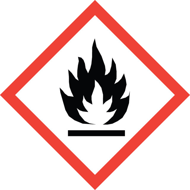

signalword
Danger
hcodes
Hazard Classifications
Eye Irrit. 2 - Flam. Liq. 2 - STOT SE 3
target_organs
Central nervous system
Storage Class
3 - Flammable liquids
wgk
WGK 1
flash_point_f
53.6 °F - closed cup
flash_point_c
12 °C - closed cup
Choose from one of the most recent versions:
Already Own This Product?
Find documentation for the products that you have recently purchased in the Document Library.