Skip to Content
Merck
CN
All Photos(1)

Documents

Safety Information

651486

Sigma-Aldrich

Gallium arsenide

(single crystal substrate), <100>, diam. × thickness 2 in. × 0.5 mm

Sign Into View Organizational & Contract Pricing

Synonym(s):
Gallium monoarsenide
Linear Formula:
GaAs
CAS Number:
Molecular Weight:
144.64
EC Number:
MDL number:
UNSPSC Code:
12352300
PubChem Substance ID:
NACRES:
NA.23

Quality Level

form

(single crystal substrate)

resistivity

≥1E7 Ω-cm

diam. × thickness

2 in. × 0.5 mm

density

5.31 g/mL at 25 °C (lit.)

semiconductor properties

<100>

SMILES string

[Ga]#[As]

InChI

1S/As.Ga

InChI key

JBRZTFJDHDCESZ-UHFFFAOYSA-N

Looking for similar products? Visit Product Comparison Guide

Physical properties

Mobility >=4500 cm2 · V-1 · S-1
Undoped (Si-type semiconductor), EPD < 5 × 104 cm-2, growth technique = LEC & HB

Physical form

cubic (a = 5.6533 Å)

Pictograms

Health hazard

Signal Word

Danger

Hazard Statements

Hazard Classifications

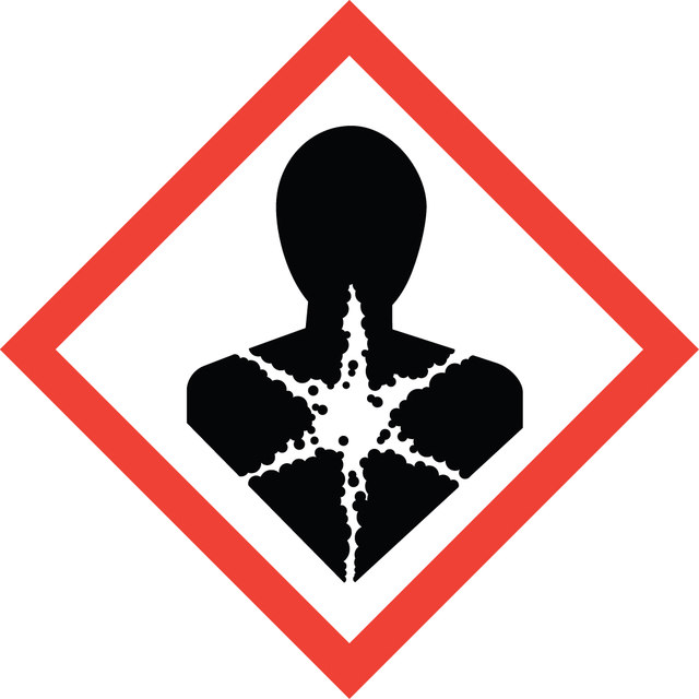
Carc. 1B - Repr. 1B - STOT RE 1

Target Organs

Respiratory system,hematopoietic system

WGK

WGK 3

Flash Point(F)

Not applicable

Flash Point(C)

Not applicable

Regulatory Information

危险化学品

Certificates of Analysis (COA)

Search for Certificates of Analysis (COA) by entering the products Lot/Batch Number. Lot and Batch Numbers can be found on a product’s label following the words ‘Lot’ or ‘Batch’.

Already Own This Product?

Find documentation for the products that you have recently purchased in the Document Library.

Visit the Document Library

Shih-Wei Tan et al.
PloS one, 7(11), e50681-e50681 (2012-12-12)
Characterization and modeling of metal-semiconductor-metal (MSM) GaAs diodes using to evaporate SiO₂ and Pd simultaneously as a mixture electrode (called M-MSM diodes) compared with similar to evaporate Pd as the electrode (called Pd-MSM diodes) were reported. The barrier height (φ(b))
Chao-Wei Hsu et al.
Nanotechnology, 23(49), 495306-495306 (2012-11-17)
GaAs is grown by metal-organic vapor-phase epitaxy on a 55 nm round-hole patterned Si substrate with SiO(2) as a mask. The threading dislocations, which are stacked on the lowest energy facet plane, move along the SiO(2) walls, reducing the number
M Baranowski et al.
Journal of physics. Condensed matter : an Institute of Physics journal, 25(6), 065801-065801 (2013-01-12)
In this study we apply time resolved photoluminescence and contactless electroreflectance to study the carrier collection efficiency of a GaInNAsSb/GaAs quantum well (QW). We show that the enhancement of photoluminescence from GaInNAsSb quantum wells annealed at different temperatures originates not
Kazuue Fujita et al.
Optics express, 20(18), 20647-20658 (2012-10-06)
Device-performances of 3.7 THz indirect-pumping quantum-cascade lasers are demonstrated in an InGaAs/InAlAs material system grown by metal-organic vapor-phase epitaxy. The lasers show a low threshold-current-density of ~420 A/cm2 and a peak output power of ~8 mW at 7 K, no
Jared J Hou et al.
ACS nano, 6(10), 9320-9325 (2012-10-02)
Ternary InGaAs nanowires have recently attracted extensive attention due to their superior electron mobility as well as the ability to tune the band gap for technological applications ranging from high-performance electronics to high-efficiency photovoltaics. However, due to the difficulties in

Articles

Spintronics offer breakthroughs over conventional memory/logic devices with lower power, leakage, saturation, and complexity.

Protocols

Photoresist kit offers pre-weighed chemical components for lithographic processes, with separate etchants for various substrate choices.

Our team of scientists has experience in all areas of research including Life Science, Material Science, Chemical Synthesis, Chromatography, Analytical and many others.

Contact Technical Service