Quantum Dots for Electronics and Energy Applications
What are Quantum Dots?
Quantum dots (QDs) are nanometer sized (~2-10 nm) semiconducting material. Owing to their small size, QDs exhibit quantum confinement effects and size-dependent electrical and optical properties. Since the discovery of cadmium based QDs in the 1980s, a variety of cadmium and non-cadmium based QDs have been synthesized and investigated. Significant improvements in the electrical and optical properties of QDs have been made by adjusting their shape and size and they have emerged as an important class of material with applications extending from light emitting diodes (LEDs), to photovoltaics, photodetectors, lasers, and field effect transistors. In this article, the properties of some of the new non-cadmium based QDs along with different applications of QDs are summarized.
Perovskite Quantum Dots
Recently discovered perovskite quantum dots with the common formula APbX3 [A = Cs, MA (methylammonium), FA (formamidinium) and X = Cl, Br, I] have attracted a lot of interest. This is mainly due to their high photoluminescence quantum efficiency (PLQY; up to 95 %) and narrow emission bandwidth (FWHM < 20-30 nm). Perovskite QDs are considered to be one of the best alternatives for CdSe based QDs. Depending upon the size and composition of the halide, the emission wavelength of CsPbX3 QDS can be tuned to cover the entire visible spectral region (from 450 to 700 nm). Figure 1 shows the colors of various perovskite QDs under UV illumination. The CsPbCl3 QDs emit blue light and the emission wavelength shifts to the green regime of visible spectrum as Cl is partially replaced by Br to yield the mixed halide perovskite CsPb(Cl/Br)3 (Figure 2). QDs with a composition of CsPbBr3 emit green light and the emission shifts towards the yellow regime for CsPb(Br/I)3 and becomes red for CsPbI3.
Among the various perovskite QDs, the one with the composition of CsPbX3 (X = Cl, Br) and emission in the range of 450-510 nm are the most stable. The enhanced optical properties and chemical robustness of these QDs make them appealing for optoelectronic applications. These cadmium free QDs, with low lead content, find applications in LEDs, backlighting in LCDs, and photodetectors.
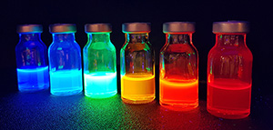
Figure 1.Colors of various perovskite quantum dots under UV illumination.

Figure 2.Emission wavelengths of perovskite quantum dots CsPbX3 (X- Cl and Br)
PBS Quantum Dots
Depending upon the size (this varies between 2.5-8nm), the emission wavelength of lead sulfide quantum dots can be tuned between 900 to 1600 nm, which falls in the infrared (IR) regime of the electromagnetic spectrum. Typically, PbS QDs exhibit a broad absorption spectrum range and narrow fluorescence bands (Figure 3). These properties make PbS QDs suitable for the use as light absorbers or infrared (IR) emitters in solar cells, for photodetectors and for infrared LEDs.
PbS quantum dots are of particular interest in solar photovoltaic applications because of their broad absorption spectrum (this extends from near infrared (NIR) to IR), high peak-to-valley ratio (>4), narrow band emission (FWHM < 100 nm) and high PLQY. These properties make PbS QDs suitable for use in tandem and multijunction solar cells for improving the efficiency of solar panels.
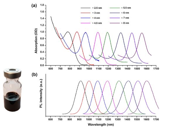
Figure 3.Absorption and emission wavelengths of ~ 4 nm PbS quantum dots.
Quantum Dot Applications
Light Emitting Diodes (LEDs)
QDs are very promising for use in light emitting layers in LED devices. The narrow emission width (defined by narrow full width at half maximum (FWHM)) and the tunability of emission wavelengths with simple variations in the size and composition make the QDs attractive for LEDs. Furthermore, the possibility of the fabrication of optoelectronic devices having QD based LEDs by roll-to-roll printing and the compatibility of most of the QDs with lightweight, flexible plastic substrates opens up the prospects for fabrication of low-cost, large-area flexible devices. Visible quantum dots-based LED is considered as a next generation display technology after OLED-displays as it exhibits high color purity, high luminance and lower power consumption.
Figure 4 shows the schematics of a QD-based LED device. First, a hole transporting layer (HTL) is spin-coated on indium tin oxide (ITO) attached to a substrate made of glass or polymer material. Then QDs are deposited by spin-coating. For visible LEDs, Perovskite, CdSe or InP based QDs are used. The PbS QDs are used for infrared LEDs. The quantum dot deposition is followed by the deposition of an electron transporting layer (ETL) and electrodes. Electrodes are typically prepared with metals such as Ag, Au, and Al and are deposited using a thermal evaporation system.1-6
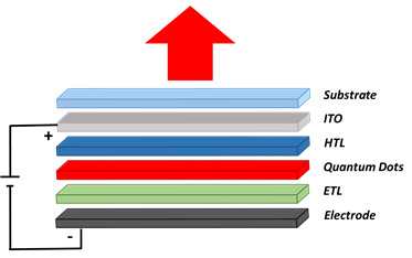
Figure 4.Sketch of a quantum dot based LED structure
Lighting
A) Liquid crystal display (LCD) backlighting
In conventional liquid crystal-based displays, the white light source from LEDs is used for backlighting. However, in the new generation LCDs, the backlighting system consists of blue LEDs and a QDs filter. The filter contains green and red quantum dots and converts the part of the blue light into green and red. Because of narrow FWHM of the resulting red, green and blue lights, it brings a wide color gamut, leading to brighter and more contrast images on LCDs. Also, this arrangement decreases energy consumption significantly. The QD-based filters can be designed in three configurations: “on-chip”, “on-edge” and “on-surface”. In the “on-chip” configuration the blend of green and red quantum dots are placed on the top of blue chip inside the LED package. In the “on-edge” configuration the blend is put inside glass rails positioned near LEDs in the package. In the “on-surface” configuration, the blend of QDs in the polymer film is integrated between the blue LEDs and the LCD matrix (Figure 5).7-11 Perovskite, CdSe-based and InP-based QDs having emission in the visible regime of the electromagnetic spectrum are useful for the backlighting application.
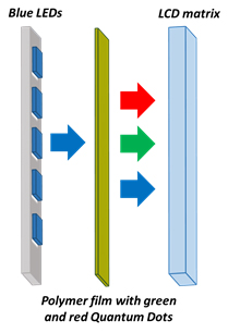
Figure 5.Schematics of Quantum Dots LCD backlighting in the “on-surface” configuration
B) Phosphors
QDs can be used as phosphors in applications such as white lighting or horticultural lighting (Figure 6). In these applications the blue LED, which is the most efficient and cheapest LED, is used as the main light source and similar to the LCD displays, QDs are used as phosphors to convert part of the blue light into another light. The possible configurations of lighting devices can be “on-chip” and “remote phosphors”. In the “on-chip” configuration the blend of QDs is placed on the top of the blue chip inside the LED package whereas in the “remote phosphor” configuration, the QDs blend in the polymer film is placed after the blue LEDs. For white lighting, the blend consists of green and red QDs. The main advantage of using QDs in white lighting is that it allows achieving a high color rendering index (CRI) and correlated color temperature (CCT). These parameters are measures of the ability of a light source to reproduce colors of various objects in comparison to a natural light source.
Red quantum dot polymer composites are promising for the use in horticultural LEDs for greenhouses for the efficient growth of plants. Plant chlorophyll is typically most efficient in capturing red (600-700 nm) and blue (400-500 nm) waves of light and the green wave is reflected. Therefore, a device with a blue LED and a polymer composite with red-emitting QDs can deliver a higher amount of photosynthetic active radiation to plants without overheating them. Use of QDs also reduces the cost of energy consumption.
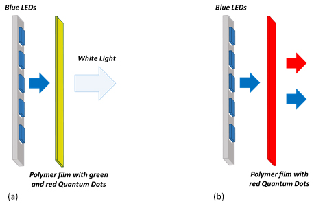
Figure 6.Cartoon of a QD based device for (a) white lighting and (b) horticultural lighting
Solar Cells
PbS quantum dots are of particular interest in solar photovoltaic applications. PbS is a semiconductor material with large Bohr exciton radius which enables quantum size-effect tuning over the range of the broad solar spectrum. Also, this material offers avenues for tandem and multijunction solar cells from a single material via size-effect bandgap tunability. Figure 7 shows a schematic of a solar cell device with QDs. PbS QDs can be of differing band gaps. Typically, the P-type PbS QDs film is deposited in a
layer-by-layer fashion by spin coating on ETL/ITO/glass substrate layers. Then the HTL and top electrode consisting of Ag or Au are deposited. Typically electrode deposition is achieved by thermal or electron beam evaporation.12-16
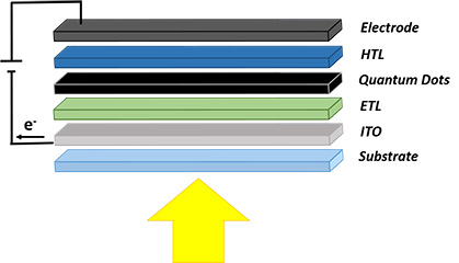
Figure 7.Schematic of a quantum dot solar cell structure
Photodetectors
QDs can be used in photodetectors for detecting both infrared and visible light. Photodetectors for infrared light find applications in night vision cameras, atmospheric spectroscopy for gas detection, biomedical imaging, quality control and product inspection. The visible light photodetectors are used in image sensors for transforming the incoming light into electronic signals. Quantum dots can also be used in surveillance, machine vision, industrial inspection, spectroscopy, and fluorescent biomedical imaging. The advantage of using quantum dots is the ease of integration with silicon electronics or with flexible organic substrates. Furthermore, quantum dots can also be deposited on prefabricated electrodes on a substrate by simple methods such as ink-jet printing, solution casting and low-temperature evaporation. The tunability of optical absorption and emission spectra through the quantum size effect is another important benefit offered by QDs. Figure 8 depicts a schematic of a QD based photodetector. Typical fabrication involves deposition of electrode on a on a glass or ceramic substrate by evaporation and then the colloidal QDs or mixture of QDs in polymers are spin-coated on the substrate to form a solid QD film or QD polymer composite between electrodes.17-18 PbS QDs are useful for photodetectors in the IR regime of the electromagnetic spectrum whereas the perovskites, CdSe and InP based QDs useful for UV-Vis regime.

Figure 8.Schematic of a quantum dot photodetectors structure
Biomedical Imaging
QDs offer several advantages as luminescent probes for biomedical imaging. These include high photostability, broad absorption spectra, large extinction coefficient, and tunable emission wavelengths. Furthermore it has been demonstrated that the surface of QDs can be modified to attach surface groups such as carboxyl, and amine to allow conjugation with biomolecules such as antibodies, polysaccharides, and peptides (Figure 9). Bio-conjugated QDs have been used as probes in DNA hybridization, receptor mediated endocytosis, monitoring of parasite metabolism, real time visualization of tissue and cellular structures, and diagnostics applications.19-21
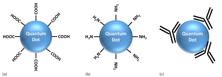
Figure 9.Cartoons representing surface functionalized QDs: (a) carboxyl functionalized, (b) amine functionalized, (c) antibody conjugated
References
如要继续阅读,请登录或创建帐户。
暂无帐户?