Perovskite Solar Cells
- Introduction
- Device Structure and State-of-the-Art
- Compositional Engineering Halide Segregation and Black Phase Stabilization
- Recombination and Passivation by 2D Perovskites
- PSC Stability: Requirements and Achievements
- PSC Stability: Aging Protocols and Field Testing
- Promises and Challenges
- Related Products
- References
Introduction
Global energy demands are steadily increasing. Estimates vary, but energy demands are expected to rise by 30% to 800 exajoules by 2040, according to the Energy Information Administration.1 Much of this demand could be supplied by the earth’s most abundant renewable energy source, solar energy. If we consider that the earth includes vast areas that receive high levels of incident sunlight, including hot, arid deserts covering tens of millions of km2, it is easy to envision that solar power has the potential to meet most, if not all, of our future energy requirements.2 However, in order to harvest this vast potential energy source, it will be critical to maximize solar cell efficiency. In order to do this, we need to both apply the new technologies that have allowed approach the 33% theoretical performance limit in single-junction solar cells, and develop efficient and low-cost materials for multijunction photovoltaics.
Lead halide perovskite solar cells (PSC) are promising candidates for meeting our growing energy needs. Single-junction PSCs can achieve conversion efficiencies of above 25% using relatively simple and inexpensive deposition methods and low purity materials, an unprecedented feat for previous photovoltaic technology. This achievement is the result of electronic properties mostly unaffected by the presence of structural defects. The chemical composition and structure of perovskites can be easily modified in order to tune the bandgap of the material. Perovskites are significantly cheaper than any other wide bandgap alternative and thus carry promise to complement silicon in tandem structures. However, in order to achieve single-junction power conversion efficiencies (PCE) higher than 26%3 PSCs require improvements to reduce non-radiative recombination. Similarly, their device long-term durability must be improved. This will require development of standardized aging protocols complemented with data from field-testing of solar cells and panels.4 Here, we discuss the latest efforts towards higher performance and stability of perovskite materials, both for single- and multi-junction solar cells.
Device Structure and State-of-the-Art
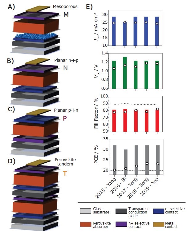
Lead halide perovskites, the most studied perovskite compositions to date, take on the 3D structure ABX3. The A cation is methylammonium (MA), formamidinium (FA), Cs or Rb. Lead sits in the B site. The halides iodine, bromine or chlorine occupy the X site. A PSC is made of a perovskite active layer, electron and hole selective materials, and transparent and/or metal electrodes. The device structure nomenclature varies based on the location of electron collection. The direct or “n-i-p” terminology applies to PSCs where the electrons are collected at the transparent interface (bottom). The inverted or “p-i-n” terminology refers to solar cells that have electron/ hole selective contacts flipped in the device stack (Figure 1). In a mesoporous structure, the bottom contact is porous: it is infiltrated and capped with perovskite material (Figure 1A). Finally, in a planar configuration all the layers tend to be compact thin films (Figure 1B and C).
PSC efficiencies increased rapidly during their first six years of development, swiftly reaching 20% and recently surpassing the 25% mark.5 Researchers have now improved control of the deposition of perovskite films and engineered the bandgap and robustness of the material in single junctions via compositional engineering.6–8 Using uniform and compact (>500 nm-thick) perovskite films and a FA-based perovskite enabled efficiencies beyond 23% with currents approaching the theoretical limit.9,10 PSCs show very high open-circuit voltages (VOC’s) compared to their bandgap, indicative of low recombination losses. Deposition, composition and device engineering have led to VOC of up to 1.24 V at a bandgap of ≈1.6 eV, with a theoretical VOC of 1.33 V for that bandgap.3 Studies have shown that recombination dynamics at the perovskite/hole selective contact interface is largely responsible for the difference between theoretical and experimental VOC’s.11 These findings prompted the study of perovskite surface passivation by 2D perovskite layers with bulky A-site cations.9,12
Early attempts at defect passivation at perovskite interfaces using thin films of wide bandgap materials enabled enhancement of the VOC of a FA-based PSC, which helped to achieve a PCE of 23.2% (certified from current-voltage curve; 22.6% certified from the a stabilized current-voltage curve).9 This achievement was followed by a report of a certified PCE of 23.3% from a stabilized current-voltage curve, warranting the exploration of new methods to identify and suppress recombination in order to boost this crucial PV parameter.13

Figure 1.Schematics of perovskite solar cells based on the A) mesoporous and B) planar, with the conducting glass/electron contact/ perovskite configuration (n-i-p). C) The inverted configuration (p-i-n) is a planar junction with a conducting glass/hole contact/perovskite stack. D) Perovskite-perovskite tandem device. E) Photovoltaic parameters of perovskite solar cells as calculated from Shockley-Queisser (bars) and metrics of selected publications (white circles) with certified efficiencies above 20% since 2015 and in chronological order to 2019.3,9,12,14,15
Compositional Engineering, Halide Segregation and Black Phase Stabilization
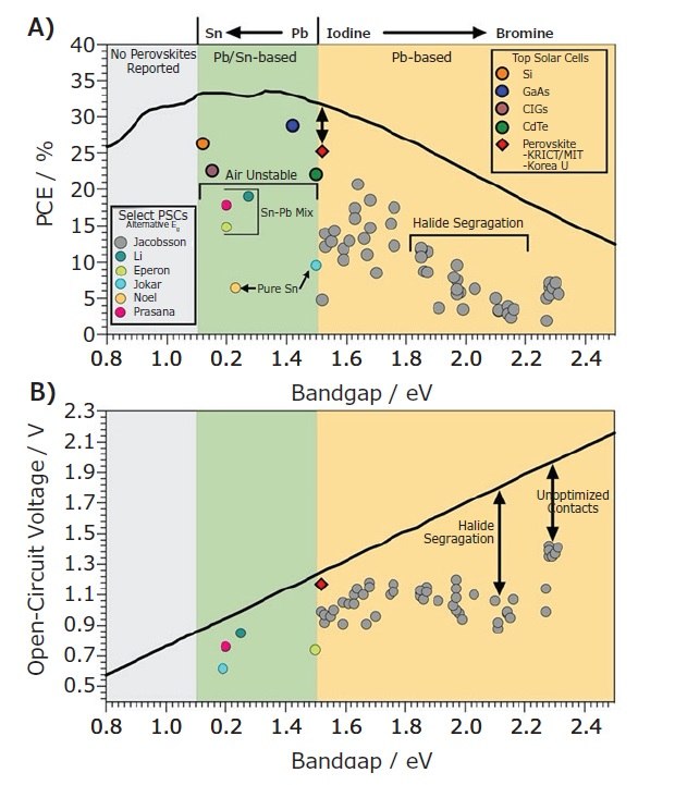
Stable 3D perovskite structures can be realized only by combining atoms with suitable steric hindrances. This requirement is quantified through the Goldschmidt tolerance factor (t), for which values between 0.8 and 1.0 result in stable 3D structures, such as in the case for MAPbI3 (t ~ 0.9). Perovskites at the edge of the tolerance factor requirement, such as FAPbI3 (t ~ 1) and CsPbI3 (t ~ 0.8), have a strained 3D lattice. As a result, they tend to form lower dimensionality photo-inactive phases at room temperature.16 Changes in the X anion have large impact on the bandgap value; increasing the Br content in an I perovskite increases the band gap closer to 1.7 eV—a value that is highly desired for perovskite/silicon tandems (Figure 1D). However, Br concentrations above 20% have raised concerns of halide segregation, possibly reducing device long-term stability and maximum VOC by forming recombination-active impurities. Mixed Sn/Pb perovskites are promising for achieving optimal bandgaps in single junctions (1.1–1.4 eV, Figure 2A), but still suffer from significant losses due to recombination. The use of complex multi-cation and anion Pb formulations has enabled researchers to avoid photo-inactive phases and reduce halide segregation in the lattice.17 A CsMAFA triple cation perovskite suppresses yellow phase impurities, even during crystallization, resulting in improved film performances regardless of annealing.18 The introduction of the smaller rubidium in RbCsMAFA has enabled 21.6% stabilized PCEs with a 1.24 V Voc for a band gap of 1.63 eV, resulting in a loss-in-potential of 390mV—one of the lowest values ever reported for any solar cell material (Figure 2B).6

Figure 2.Device photophysics of state-of-the-art PSCs with A) Shockley Queisser efficiency and B) the calculated maximum VOC (radiative limit) compared to values reached for different absorber materials.5,21–26
Following such examples, scientists have introduced other smaller cations, such as K, into solution without a clear explanation of how these positively charges atoms are incorporated; however, the presence of K+ clearly benefits the optoelectronic properties of the materials.19 More recently the mechanism of how these cations are incorporated in the perovskite lattice has been studied, providing evidence of doping by strontium.20 Cations larger than FA have been used to induce formation of lower dimensionality perovskite phases at interfaces, where the charge-transport layers are separated by the larger cations. Their larger bandgap enables passivation of surface defects, reducing non-radiative recombination and their use in devices has enabled current performance records.9,12 Pure 2D/3D perovskites, where 2D interlayers are also diffused in the bulk, have been also reported. So far, the most stable and efficient perovskite compositions have been based on the combination of multi-cation perovskites and 2D interface passivation of 3D perovskites (Figure 1E).
Recombination and Passivation by 2D Perovskites
In a real device, bulk defects and surfaces/interfaces introduce recombination centers that result in rapid non-radiative recombination. Non-radiative recombination is different from radiative recombination and causes loss in potential (VOC – bandgap/elementary charge, Figure 2B). While radiative recombination rate is a material property, non-radiative recombination is dictated by defects. Currently, interface recombination represents an obstacle for mixed-halide wide bandgap perovskites and for narrow bandgap tin-based perovskites used in multijunction solar cells stacks. Recent efforts allowed to significantly reduce interface recombination in single-junctions.27 Bulk non-radiative recombination requires further reduction for all perovskite compositions. Lack of carrier selectivity, barriers to charge extraction and surface defects at interfaces are main causes of surface recombination. Other research has reported non-radiative recombination at grain boundaries in perovskite films, along specific crystallographic facets, and in the presence of porosity in the film, although this still remains a debated topic.28 Bulk recombination in PSCs has been attributed to electron-phonon coupling, band electronic disorder (higher Urbach energy) and deep-defects (both intrinsic and induced by impurities). To reach VOC,rad, and in turn, to also maximize the FF to nearly 90%, investigators will need to minimize the impact of such defects, with the goal of approaching 10 μs non-radiative lifetimes.27
PSC Stability: Requirements and Achievements
The key cost drivers of new solar technology include capital expenditures as well as energy yield, which is a product of device efficiency and long-term stability. The degradation of the PCE over time controls the return on investment and thus, the risks associated with a new PV technology. The market reference for solar technology is crystalline silicon, with a degradation rate below 0.5% per year, delivering performance for 25 years under operational conditions. PSCs must reach similar levels of stability to compete within the photovoltaic market.
A significant body of research has been devoted to this aim in the last few years, with significant efforts directed to reducing the impact on stability of both intrinsic and extrinsic degradation factors. Despite initial scepticism, perovskite solar cells can now withstand the damp-heat and temperature-cycling protocols used for accelerated aging in the silicon industry (IEN6125).29 Milestones in this progress have provided effective design of each of the device layers and interfaces, and the development of effective encapsulation techniques.29 The impact of extrinsic degradation factors, such as temperature, or chemically active species as humidity and oxygen, and the release of perovskite degradation by-products have been minimized, halting further material degradation.29,30 More recently, inorganic device structures have started to attract attention: a stable photovoltaic β-phase has been discovered at room temperature for CsPbI3, raising efficiencies above 10%. Combined with inorganic interlayers, such compositions promise to overcome the low-stability issue of perovskite photovoltaics.30
PSC Stability: Aging Protocols and Field Testing
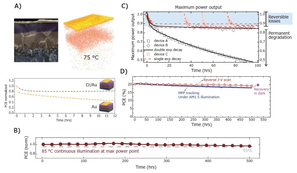
Perovskites fall subject to ion migration, which partake in both fast (seconds to minutes) and slow (minutes to hours) performance degradation, namely hysteresis and reversible losses (Figure 3A-D). In the latter, devices suffer from decreased PCE during aging and recover to the initial value after dark storage for a few hours. Consequently, a true estimation of device lifetime becomes complex, and easily prone to over or under estimation. Even simple figures of merit as T80 can be misleading, depending on how they are reported. Regardless, establishing how organic and inorganic contacts affect the accumulation of ions in the long term proves critical, as mild, reversible losses does not guarantee long-term stability. Suitable characterization protocols need to be developed to correlate stress factors and device degradation, to enable further improve device stability. Following the example of organic photovoltaics, researchers have attempted to craft characterization guidelines for perovskite devices by complementing the International Summit on Organic Photovoltaic Stability (ISOS) protocols with further measurements aimed at assessing the impact of ionic motion on device stability. They further defined reporting standards to truly enable the implementation of round robin experiments on published devices. A formatted reporting of such data, their integration in databases, and their correlation through machine learning algorithms, would contribute to a better understanding of the current limiting factors for device stability.31 As the field develops, more field-testing data from solar cells and panels are expected to be published. The study of the observed failure mechanisms and their correlation with the ones observed in the accelerated aging protocols will enable further improve the aging standards and to correlate such results with expected device lifetimes.31

Figure 3.Long-term stability of perovskite solar cells. A) Gold migration-induced PCE degradation under light, maximum power point and 75 °C. It can be offset by a Cr interlayer between Spiro-OMeTAD and the gold electrode.32 B) The use of multiple cations and a PTAA hole contact shows losses around 5% in 500hrs of MPP tracking at 85 °C, in a mesoporous device.33 C) Maximum power output in real working conditions shows reversible losses before going through permanent degradation.34 D) One of the most stable planar devices exhibited losses around 10% in 500 hrs of MPP tracking at room temperature.35
Promises and Challenges
PSCs have made remarkable advances in just a few years — a result of both the scientific community’s extensive efforts and expertise developed in more established fields, such as organic or dye-sensitized solar cells. The above 25% lab-scale efficiency and the remarkably low loss-in-potential recently reported by PSCs show that these solution-processed solar cells are ready to rival other state-of-the-art technologies, such as Si or GaAs. Having reached the single-junction efficiency target, the focus of the perovskite community has now shifted towards tandem solar cells and long-term stability. The perovskite community is trying to develop testing protocols able to account for the unique dynamics of these materials. First reports simulating outdoor field-testing have recently been published, but more data are required to provide statistical robustness and to confirm the validity of the proposed aging protocols.36 To become a player in the energy market, PSCs must be able to last for at least 20 years with minimal degradation. Scientists can only accomplish this task by mitigating intrinsic and extrinsic degradation due to ion migration in the perovskite device stack.
References
To continue reading please sign in or create an account.
Don't Have An Account?