Van der Waals Heterostructures: Synthesis & Apps
Introduction
Van der Waals heterostructures (vdWHs) are synthetic quantum systems composed of atomically thin layers. Traditional semiconducting heterostructures require components with similar crystal structures; this strict lattice matching becomes less critical in vdWHs due to the weak (van der Waals) interaction between two adjacent planes.1 Fabrication of these 2D vdWHs occurs via sequentially stacking (mechanical transfer) or direct growth (chemical/physical vapor deposition).2 Moreover, the features in vdWHs are decided not only by the constituents but also by the relative crystallographic alignment; their physical properties can be further controlled or improved through electrostatic gating and strain engineering.1,2 The emergence of two-dimensional (2D) layered materials ranging from graphene, hexagonal boron nitride (h-BN) to molybdenum disulfide (MoS2) provide versatile fundamental building blocks for many new types of vdWHs. As the field of 2D materials expands, vdWHs exhibit many new potential applications in next-generation electronics and optoelectronics, such as memories, light-emitting diodes (LEDs), and photodetectors.3
When a 2D material is wrapped into a cylinder, the resulting nanotube exhibits some exciting functionalities since it combines the characteristics of both 2D and 1D materials such as diameter-dependent bandgap in carbon nanotubes (CNTs). This provides opportunities to create radial heterostructures such as 1D vdWHs.4 For instance, cylindrical 2D materials are being explored as single-photon emitters in nanophotonic circuitry due to the strong edge state effect on the optoelectronic properties.5 Crystalline MoS2 layers coated on CNTs as a conductive backbone can be applied to battery electrodes because MoS2 channels offer more active lithium-ion intercalation sites.6 1D vdWHs are a burgeoning research field, and the recent achievements and development of on these hybrids are significant.
This review presents the most recent research activities on 1D vdWHs, including the candidate materials, the synthetic techniques, and characterization methods. The optoelectronic applications are discussed in detail for different constructions of the 1D vdWHs-based devices (FETs, sensors, LEDs, photovoltaic devices, and light detection). Some challenges and perspectives for future development and applications of 1D vdWHs are also proposed to conclude the review.
Potential van der Waals Materials
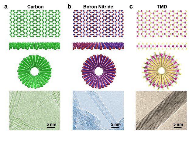
Both CNTs and graphene contain exceptional mechanical and electrical characteristics and are potential van der Waals materials. CNTs were first reported in 1991 by S. Iijima;7 CNTs include single-layered nanotubes, which are commonly referred to as single-walled carbon nanotubes (SWCNT). Graphene, an allotrope of carbon consisting of a single layer of atoms arranged in a two-dimensional honeycomb lattice, came onto the scene more recently than CNTs. In this case, a CNT can be thought of as a sheet of graphene (Figure 1A) rolled into a cylinder. Intrinsic graphene is a zero-band-gap semiconductor; however, CNT exhibits metallic or semiconducting behavior (0~2 eV), as determined by the rolling direction and radius (chirality). This striking modification of the electronic state by rolling into a tube with periodic boundary conditions made SWCNT a unique nanomaterial. Both show various applications in electronics, batteries, sensors, and more.4
The crystal texture of hexagonal boron nitride (h-BN, Figure 1B) is similar to graphite, where strong covalent bonds bind boron and nitrogen atoms in-plane, with adjacent layers coupled via van der Waals forces. Boron atoms lie over and above nitrogen atoms, responsible for the polarity of the B-N bonds. Boron nitride nanotubes (BNNTs), experimentally discovered in 1995, display electrically insulating properties with a bandgap of ~5.5 eV, independent of tube chirality and morphology. BNNTs have physicochemical features that allow for potential medical and biomedical applications, including gene delivery, drug delivery, and neutron capture therapy.8
In 1992 discovery of transition metal dichalcogenide (TMD) nanotubes, like MoS2 (Figure 1C), stimulated intense experimental and theoretical research of other fascinating inorganic tubular structures. Many TMDs are semiconductors (with tunable band-gaps from ~1–2 eV, depending on the layer thickness), and research on 2D TMDs, demonstrates a transition from indirect band-gap to direct band-gap when the thickness reduces to a monolayer.3 All these unique features, combined with appreciable charge mobility, make TMD materials promising candidates for high-performance optoelectronics.1

Figure 1.Crystal Structures of representative 2D van der Waals materials: A) carbon, B) boron nitride, C) MS2, where M = Mo, W, etc. and their corresponding tubular counterparts that have been experimentally evidenced.
Synthesis and Assembly Techniques
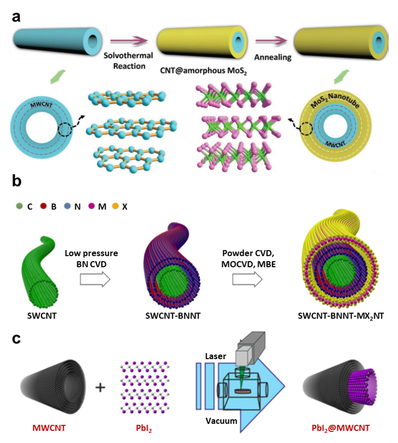
CNTs and BNNTs are produced via well-established techniques, including arc-discharge, laser ablation, and chemical vapor deposition. But there were only a few reports on the successful production of other tubular structures (e.g., TMDs) using these synthetic approaches. An alternative route has focused on using a tubular template such a as CNT to facilitate atom packing: Figure 2A presents a solvothermal process to realize the 1D vdWHs.9 Here, amorphous MoS2 sheath wrapped around the CNT serves as an intermediate coating on CNTs and allows conversion into crystalline sheets upon thermal annealing. Removal of residual particles that can lead to scattering of electrons and photons is required when using the precursors in the solution method. When using a solvent-free high-temperature route, experiments have produced SWCNT@BNNT, SWCNT@MoS2NT, and even a ternary SWNT@BNNT@MoS2NT (Figure 2B).10 Each layer shows single-crystalline nature, and different van der Waals cylinders are coaxially nested, confirming an open-end growth mechanism contributes to the formation process.4 For these as-prepared vdWHs, the active materials or the target nanotube sits outside the template, exposed to a foreign environment, where some materials may be unstable or even become damaged. As a result, efforts are also focussed on confining the formation of the second phase to the tubular template. In previous dry or wet methods, the nanotube ends must remain open, and a long-term thermal annealing process is required to facilitate precursor penetration.11 Tobias and colleges presented a laser-assisted strategy (Figure 2C) for cylindrical vdWHs, allowing the encapsulation of single-layered lead iodide into the cavities of CNTs.12 More importantly, the carbon shell protected the air-sensitive lead iodide, and the cylindrical vdWHs were able to be directly manipulated under ambient conditions.

Figure 2.A) Schematic representation of the solvothermal synthesis process of coating crystalline MoS2 layers onto CNTs. Reprinted with permission from reference 9, copyright 2016 WILEY-VCH Verlag GmbH & Co. KGaA, Weinheim. B) Sketch shows the solvent-free high-temperature route of a SWCNT-BNNT-MX2NT 1D vdWHs. Reprinted with permission from reference 4, copyright 2021 American Association for the Advancement of Science. C) Illustration of the laser-assisted filling of multiwalled carbon nanotubes. Reprinted with permission from reference 12, copyright 2018 American Chemical Society.
Characterization of 1D vdWHs
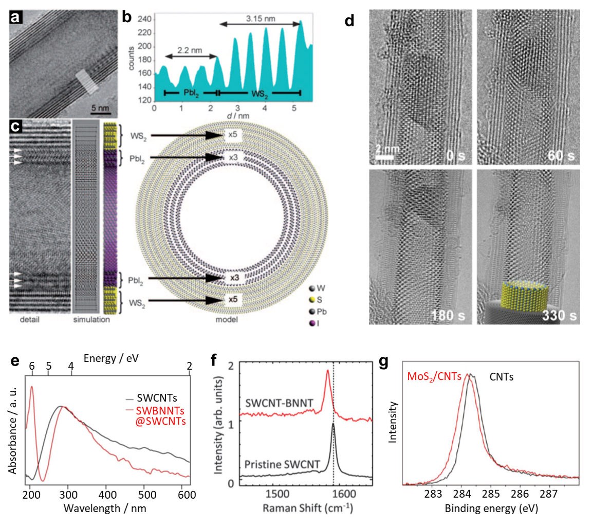
Obtaining the structural information of 1D vdWHs, is essential, particularly near the interface, this is primarily obtained through high-resolution transmission electron microscopy (HRTEM) typically by employing spherical aberration correction. In a typical HRTEM image (Figure 3A), PbI2 layers are conformably encapsulated in the inner core of the host WS2 nanotubes (Figure 3B).8 The two phases can be distinguished via different layer distances (Figure 3C).15 Electron microscopy with adjustable irradiation offers a powerful tool to uncover the growth dynamics of the 1D vdWHs, i.e., the formation of a PbI2 nanotube in such a confined geometry (Figure 3D), where a continuous blending of the nanorod onto the nanotube has been directly evidenced.14
The optoelectronic properties of 1D vdWHs can be modulated because carriers (holes and electrons) in the atomically thin layers are exposed to layer-to-layer coupling.1 The absorption spectrum of BNNT@SWCNT (Figure 3E) presents a new peak emerging at 6.1 eV compared to that of pristine CNTs, associated with π-π* bands of the BNNTs.15 Meanwhile, a blue-shift (5–10 cm-1) of the G band (relative to CNT) has been demonstrated in the BNNT@SWCNT vdWHs, using Raman characterization (Figure 3F); a possible explanation for this shift is the thermal strain between BNNT and CNT.4 As to the X-ray photoelectron spectroscopy (XPS) spectrum of MoS2NT@CNT vdWHs (Figure 3G), a downshift of the C 1s line by 0.15 eV appears as compared with the pristine CNTs, attributed to a decrease in the Fermi level energy led by the p-doping of CNTs.16 Although not fully documented yet, there should be strong electronic and excitonic coupling between different nanotubes in a 1D vdWH. The precise understanding of the characterization and evaluation of those vdWHs is significant for their further applications once their dimension is down to 1 nm.

Figure 3.A) HRTEM micrograph showing a core-shell PbI2@WS2 composite nanotube. B) Line profile obtained from the indicated region in-plane (A); C) the complex contrast of the inner PbI2 layers (arrowed) relative to the outer WS2 layers. Reprinted with permission from reference 13, copyright 2016 Wiley-VCH Verlag GmbH & Co. KGaA, Weinheim. D) Sequence of images showing the transformation from a nanorod fragment onto a single-layered nanotube, cyan, green and grey spheres representing Pb, I and C atoms, respectively. Reprinted with permission from reference 14, copyright 2016 WILEY-VCH Verlag GmbH & Co. KGaA, Weinheim. E) Absorption spectroscopy of SWCNTs and SWBNNT@SWCNTs. Reprinted with permission from reference 15, copyright 2016 Springer Nature. F) Raman presents typical G band of an individual SWCNT before and after BN coating. Reprinted with permission from reference 4, copyright 2021 American Association for the Advancement of Science. G) XPS C 1s spectra of pristine CNT sample and MoS2/CNTs composite. Reprinted with permission from reference 16, copyright 2011 American Chemical Society.
Potential Applications
Semiconductor heterostructures are considered the base of modern optoelectronics, specifically for LEDs and solar cells.2 1D vdWHs with radially modulated compositions/band-gaps provide a platform for a deep understanding of the hetero interface and have shown great potential for various semiconductor systems, such as high mobility transistors, chemical sensors, photodetectors, and photovoltaic cells.11,14 The reduced dimension of the vdWHs (down to 1D level) creates challenges for manipulating these samples during device fabrication.17 Here, we briefly discuss the 1D vdWH-based optoelectronic devices available currently or in the near future.
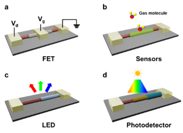
First, we will examine field-effect transistors (FETs), schematically illustrated in Figure 4A, where the conductive channel (CNT) can be completely isolated by the dielectric layer (BNNT). High mobility is expected because the free surface dangling bonds lead to a significant carrier scattering reduction,3 but an appropriately thick dielectric layer is required to prevent gate leakage.12 In addition, the high thermal stability of both SWCNT and BNNT, makes these transistors appealing for creating durable commercial integrated circuits.
Chemical sensors based on 2D vdWHs for detecting various gases, such as nitrogen dioxide (NO2) and ammonia (NH3), rely on the capture/release of free electrons at the semiconductor surface.2 This is also the base principle for 1D vdWHs (Figure 4B). Once exposed to the target gas molecules (e.g., NO2), the change in carrier density of the outer shell (MoS2) modulates the transport in the core channel (e.g., CNT) via the surface gating effect. Due to the large interfacial area, sensitivity as low as ppm level may be achieved, vital for environmental monitoring systems.
The core-shell geometry enables a low recombination rate and a high efficiency of charge collection, principally attributed to shortened migration paths for the minority carriers.18 This makes coaxial junctions established on type-II band alignment, like P-N or metal-insulator-semiconductor heterojunctions (e.g., p-CNT/BNNT/n-MoS2), practical for high-efficiency light-emitting (Figure 4C) or photovoltaic devices. Note that careful energy band matching is required since the band bap of SWCNT strongly depends on its chirality. In cylindrical heterostructures like these, a strong polarization dependence may be observed due to crystal anisotropy one interesting result is that LEDs based on 1D vdWHs could be used for integrated optoelectronics due to their small diameters.
The vdWHs discussed here provide more tunability for band alignments and carrier densities and have shown promising applications in high-performance photodetectors. Previous work has shown that position control of the heterojunctions within an individual tube (with different optical band gaps), opens the door for multispectral or broadband sensing (Figure 4D).12 This makes possible an entire spectroscopy system within an individual tubular structure, rendering a path to miniaturized spectroscopic applications.19

Figure 4.Schematic diagrams of a device using the 1D vdWHs: A) a “gate-all-around” field-effect transistor, B) a chemical or biological sensor, C) LED, D) broadband spectrum photodetector.
Challenges, Outlook, or Prospect
VdWHs based on low-dimensional materials have seen significant development in recent years due to their strong localized states at the submicron scale. Here, we present a brief review of 1D vdWHs, including the candidate materials, synthetic routes, characterization methods, and potential applications, including transistors, chemical sensors, LEDs, and photovoltaic devices photodetectors. However, compared with the 2D vdWHs, 1D vdWHs have yet to attract significant attention, although research is beginning to show their significant potential for next-generation integrated circuits. The controllable preparation of 1D vdWHs is indispensable. Sub-mm-large 2D vdWHs can be obtained either by transfer or direct growth. Fabrication of long and perfect coaxial junctions will be imperative for advancing new studies. While the CVD method can grow high-quality single crystals, there is still a technical challenge to preparing ultralong 1D vdWHs due to low efficiency of the gas-feeding-dominant process. At the current stage, high growth temperate (>1000 °C) and the vacuum environment hinder industrial production. Further work should balance the reaction temperature and the growth efficiency; a catalytic assisted route may be feasible. Second, the number of materials appropriate for 1D vdWHs (mainly CNT, BNNT, and MoS2) is too few compared to 2D vdWHs. The rising PbI2 indicates a possible supplement. Another challenge is the precise control of inner and outer atomic arrangements, and chirality or polarity in a tubular structure. It may be interesting to fabricate 1D vdWHs using chirality-free templates. The decrease in 1D vdWHs’ dimension (less than 1 nm) may also requires new theoretical work given the strong quantum effect and the inter-tube coupling.[i] In summary, 1D vdWHs are an essential conceptual novelty in the materials community and only the persistent exploration of 1D vdWHs will fulfill their promising application in next-generation optoelectronics.
Acknowledgments
RX, QZ contributed equally to this work. Part of this work was supported by JSPS KAKENHI (grant numbers JP18H05329, JP19H02543, JP20H00220, 20K14660, and JP20KK0114) and by JST, CREST grant number JPMJCR20B5, Japan. Part of the work was conducted at the Advanced Characterization Nanotechnology Platform of the University of Tokyo, supported by the “Nanotechnology Platform” of the MEXT, Japan, grant number JPMXP09A20UT0063.
Materials
References
To continue reading please sign in or create an account.
Don't Have An Account?